
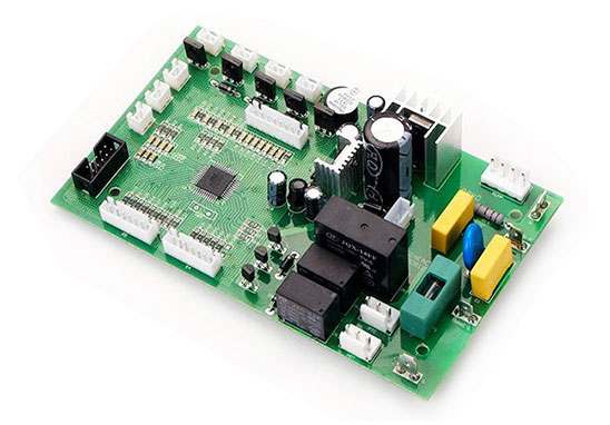
Professional PCB manufacturing and assembly
Building 6, Zone 3, Yuekang Road,Bao'an District, Shenzhen, China
+86-13410863085Mon.-Sat.08:00-20:00

Short circuit is a common machining defect in the manual welding process of SMT. In order to achieve the same results between the manual patch and the machine patch, the short-circuit problem must be solved. If the PCBA circuit board is short-circuited, it should never be used. There are many ways to solve the problem of short circuit in SMT chip processing. Next, Shenzhen PCBA processing manufacturer -kingford will introduce the method to prevent short circuit in SMT chip processing.
Method of preventing short circuit in SMT patch processing
1, manual welding operation to form a good habit, with a multimeter to check whether the key circuit short circuit, each time after the manual SMT patch an IC need to use a multimeter to measure whether the power supply and ground short circuit.
2. Light the short-circuit network on the PCB drawing, look for the most tolerant place of short-circuiting on the circuit board, and pay attention to the IC internal short circuit.
3. If the same short circuit occurs in batches during SMT patch processing, you can take a board for sectioning operation, and then energize each part respectively to check the short circuit part.
4. Use short-circuit positioning analyzer for inspection.
5, if there is a BGA chip, because all the solder joints are covered by the chip can not be seen, and it is a multilayer board (4 layers above), so it is best in the design of the power of each chip is divided, with a magnetic bead or 0 ohl resistance connection, so that when the power supply and ground short circuit, disconnect the magnetic bead detection, it is easy to locate a chip.
6, small size SMT patch processing surface paste capacitor welding must be careful, especially power filter capacitor (103 or 104), the number is large, it is easy to cause short circuit between the power supply and the ground.
PCBA processing advantages
1. Highly professional: The company focuses on processing samples and small and medium-sized batches, and promises to deliver the materials within 3-5 working days after confirmation.
2. Professional equipment: The company's equipment is tailored for sample and small and medium-sized batch production of advanced equipment, can stick 0201, BGA spacing 0.3MM, QFN, CSP, CON and other components.
3. Professional technology: 100% of technical backbone workers have more than 5 years of work experience, 85% of front-line operators have more than 3 years of work experience.
4. The company implements the 5S and 6σ concepts in daily operation, so as to ensure that the shipment is checked at least 7 times. If the quantity reaches 100PCS, our company promises to pass AOI optical inspection.
5. The company promises that the straight through rate of welding is more than 99%. If customers find welding defects, the company promises to repair them free of charge.

2. How to reduce the impact of PCB stray capacitance?
The term often used when referring to electronic circuits on PCbas is stray capacitance. Stray capacitance may exist between conductors on PCBS, prefabricated circuit boards of passive devices, PCbas, boards with mounted components, and SMD component kits in component packages (especially IC). Stray capacitance is one of the inherent physical properties of electronic circuit and circuit board. So how to reduce the impact of PCB stray capacitance?
PCB design method to reduce stray capacitance of PCB
1. Remove the inner stratum
PCBS are designed because grounding strata increase capacitance to adjacent conductors due to proximity, so it helps to remove the inner grounding strata to increase distance, which minimizes capacitance effects. This must be weighed against minimizing the EMI benefits obtained when the ground plane is adjacent to the signal plane.
2. Use the Faraday Shield
A Faraday shield is a grounded trace line or plane placed between two trace lines that the PCB is designed to minimize the capacitance effect between them, and like other shield structures, it can effectively reduce stray capacitance.
3. Increase the space between adjacent tracks
Another effective mitigation technique is PCB design that increases the spacing between adjacent tracks. As the capacitance decreases with distance, this is a very good method that can be applied.
4, minimize the use of holes
The through-hole is the key element that makes compact, complex PCBS possible. However, overuse can increase the parasitic capacitance problem. Stray capacitance, for example. This PTH coupling can be reduced by a PCB design that eliminates annular loops around the perforations on unconnected layers and minimizes the number of perforations from the components. Such as BGA.
Why choose Shenzhen kingford?
1. Strength guarantee
▪SMT workshop: We have imported SMT machines and several sets of optical inspection equipment, with a daily output of 4 million. Each process is equipped with QC personnel, who can keep an eye on product quality.
▪DIP production line: We have two wave-soldering machines, among which there are more than 10 old employees who have worked for more than three years. The skilled workers can weld all kinds of plug-in materials.
2. Quality assurance, cost-effective
▪ High-end equipment can stick precision shaped parts, BGA, QFN, 0201 materials. Can also template patch, loose material hand.
▪ Sample and size batch can be produced, proofing from 800 yuan, batch 0.008 yuan/point, no start-up fee.
3. Rich experience in SMT and welding of electronic products, stable delivery
▪ Accumulated SMT SMT processing services for thousands of electronic enterprises, involving many kinds of automotive equipment and industrial control motherboard. The products are often exported to Europe and the United States, and the quality can be affirmed by new and old customers.
▪ On time delivery, normal 3-5 days after complete materials, small batch can also be expedited on the same day shipment.
4. Strong maintenance ability and perfect after-sales service
▪ Experienced maintenance engineers can repair all kinds of patch welding caused by bad products, to ensure the connection rate of each piece of circuit board.
▪ 24-hour customer service staff at any time response, the fastest speed to solve your order problems.
What are the PCBA board repair requirements?
Mar 07,2023


Just upload Gerber files, BOM files and design files, and the KINGFORD team will provide a complete quotation within 24h.