
Professional PCB manufacturing and assembly
Building 6, Zone 3, Yuekang Road,Bao'an District, Shenzhen, China
+86-13410863085Mon.-Sat.08:00-20:00

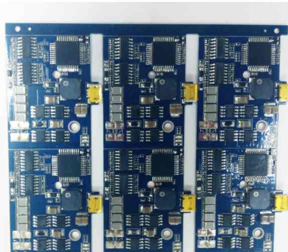
In PCB production process, there is a relatively important process, that is, process edge. The reservation of process edge is of great significance for the subsequent SMT patch processing. Next, Shenzhen PCBA processing manufacturers to introduce the role of PCB process edge, production methods and design requirements.
PCB process edge role
The process edge is the part added on both sides or four sides of the PCB board, mainly to assist the SMT plug-in to weld off the board, that is, to facilitate the SMT SMT machine track clamp the PCB board and flow through the SMT SMT machine. If the components too close to the track edge absorb the components in the SMT SMT machine nozzle and attach them to the PCB board, the collision phenomenon may occur. As a result, production cannot be completed, so a certain process edge must be reserved, with a general width of 2-5mm. This method is also suitable for some plug-in components, after wave soldering to prevent similar phenomena.
The process edge is not a part of the PCB board and can be removed after the PCBA manufacturing is completed.
PCB process edge production method
1, V-CUT: a process connection between the process edge and the board, slightly cut on both sides of the PCB board, but not cut!
2, connecting bars: use several bars to connect the PCB board, make some stamp holes in the middle, so that the hand can be broken or washed off with the machine.
PCB process edge design requirements
Not all PCB boards need to add process edge, if the PCB board space is large, leave no patch components within 5mm on both sides of the PCB, in this case, there is no need to add process edge, there is also a case of pcb board within 5mm on one side of no patch components, as long as add process edge on the other side. These need the attention of PCB engineer.

PCB process edge function, production method and design requirements
The board consumed by process edge will increase the overall cost of PCB, so it is necessary to balance economy and manufacturability when designing PCB process edge.
For some special shape PCB board, the PCB board with 2 or 4 process edges can be greatly simplified by cleverly assembling the board.
In the SMT processing, the design of the piecing mode needs to take full account of the track width of the SMT piecing machine. For the piecing board with a width exceeding 350mm, it is necessary to communicate with the SMT supplier's process engineer.
2. Advantages and disadvantages of PCB surface treatment process OSP
OSP is organic welding film, also known as copper protection agent, which is mainly exposed to the air of copper to play a certain protective role, which is a common surface treatment process in PCB processing. Everything is not perfect, OSP is no exception, the next Shenzhen PCB board factory - kingford to introduce the advantages and disadvantages of PCB board surface treatment process OSP.
The role of OSPs
OSP acts as a barrier between copper and air. This is the difference with other surface treatment processes. OSP is organic matter, not metal, so it is cheaper than tin-spraying process. The principle is to grow a layer of organic film on a clean surface of bare copper by chemical method. Many computer motherboards use OSP process.
This layer of organic film can make the circuit board before welding to ensure that the inner layer of copper foil will not be oxidized, welding, once heated, this film will evaporate, the solder can weld the copper wire and components together.
Advantages and disadvantages of OSPs
Advantages:
With all the advantages of bare copper plate welding, expired plates can also be re-finished.
Disadvantages:
1, OSP transparent colorless, more difficult to check, it is difficult to identify whether the OSP treatment.
2, the OSP itself is insulated, non-conductive, will affect the electrical test. In this way, the test point must open the steel mesh and solder paste to remove the original OSP layer, in order to contact the needle point for electrical testing. Osps cannot be used to handle electrical contact surfaces, such as keyboard surfaces for keystrokes.
3, OSP is not corrosion resistant, easy to be affected by acid and temperature. When used for secondary reflow welding, it should be completed within a certain time, usually the second reflow welding effect will be poor. If the storage time is more than three months, it must be resurfaced and used up within 24 hours after opening the package.
An OSP circuit board, exposed to the air for ten days, will not be able to weld components.
kingfordPCB board making ability
Energy production from 2 layers to 14 layers, 14-22 layers can be proofing production.
Minimum line width/spacing: 3mil/3milBGA Spacing :0.20MM
Minimum aperture: 0.1mm Size :610mmX1200mm
Ink: Tamura, Taiyo, Fudoken;
FR4: Shengyi, Kingboard, Harbour, Hongren, Guoji, Hezheng, Nanya,
(Shengyi S1130/S1141/S1170),Tg130℃/ Tg170℃ T g180℃ and other high TG plates)
High frequency plate: Rogers, Taconic, ARLLON;
Surface process: tin spray, lead-free tin spray, gold plating, full plate gold plating, plug gold plating, full plate thick gold, chemical tin (silver), anti-oxidation (OSP) blue glue, carbon oil
Shenzhen kingford is a professional manufacturer of printed circuit board manufacturing, 20 years focused on single, double-sided, multi-layer circuit board production. We can provide PCB proofing and mass production services such as FR4 hard board, FPC soft board, HDI board and metal substrate.
Common wiring rules for PCB design
Feb 25,2023


Just upload Gerber files, BOM files and design files, and the KINGFORD team will provide a complete quotation within 24h.