
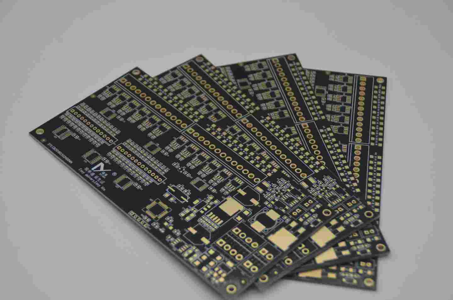
Professional PCB manufacturing and assembly
Building 6, Zone 3, Yuekang Road,Bao'an District, Shenzhen, China
+86-13410863085Mon.-Sat.08:00-20:00

With the development of miniaturization of electronic products and high-density assembly of circuit board components, SMT production and testing have brought great challenges. From the detection method, it can be subdivided into: Manual visual, digital microscope, SPI solder paste detector, automatic optical detection (AOI), SMT first piece detector, online test (ICT minute needle bed, flying needle), functional test (FCT), automatic X-ray detection (X-ray or AXI) and other methods, the above main SMT detection technology is briefly introduced.
One. SPI solder paste detector
SPI solder paste detector uses the principle of optics and calculates the height of solder paste printed on PCB board by triangulation. Its function is to detect and analyze the quality of solder paste printing, discover SMT process defects in advance, allow users to monitor the problems in production in real time, reduce the defects caused by solder paste printing, and provide operators with strong quality control support. Enhance process performance.
Two, manual eye inspection
Manual eye inspection is the use of human eyes with or without lighting magnifying glass, with the naked eye inspection of printed circuit boards and solder joints appearance, missing parts, wrong parts, polarity reverse, offset, tablet and other aspects of quality problems.
Three, digital microscope
Digital microscope is the microscope to see the image of the object through digital to analog conversion, it will be the image of the object enlarged and displayed on the computer screen, you can save the picture, enlarge, print. Measuring software can measure all kinds of data. It is suitable for the inspection of electronic industry production line, the detection of printed circuit board, the detection of welding defects in printed circuit components, etc.
Four, SMT first piece detector
Through intelligent integration of CAD coordinates, BOM list and first PCB scan, the system can automatically input the measurement data, thus simplifying the inspection of the first piece of SMT production line. LCR can automatically read the data corresponding to the corresponding position and judge the test result automatically. Avoid false test and leakage test, and automatically generate test reports stored in the database test reports stored in the database.
Five, AOI automatic optical inspection
AOI (Automated Optical Inspection) is a new type of automatic optical inspection technology, which uses optical and digital imaging technology, and uses computer and software technology to analyze images.
AOI equipment can be generally divided into online (in the production line) and off-line two categories.
AOI detection is a kind of detection technology formed by the integration of computer technology, high-speed image processing and recognition technology, automatic control technology, precision machinery technology and optical technology.
AOI automatically scans PCB circuit board through the camera, collects images, compares the solder joints tested with qualified parameters in the database, and checks the defects on PCB through image processing: Missing parts, wrong parts, bad parts, tin ball, offset, side stand, monument, reverse paste, pole reverse, bridge connection, virtual welding, no solder, less solder, more solder, component float, IC pin float, IC pin bending, and through the display or automatic signs to show/mark the defects, for maintenance personnel repair.
Six. X-ray Detection (X-ray or AXI for short)
AutomaticX-ray detection AXI(AutomaticX-raylnspection)
X-Ray detection is the use of X-ray penetration and attenuation properties in the substance to find defects, mainly detect internal defects of solder joints, such as BGA, CSP and FC Chip solder spot detection.
X-ray detection is the use of X-ray has a strong penetration, can penetrate the surface of the object performance, perspective is inspected solder joint internal, so as to achieve the detection and analysis of various common solder joint welding quality of electronic components.
X-Ray detection can fully reflect the welding quality of the solder joint, including open circuit, short circuit, holes, holes, internal bubbles and insufficient tin, and can achieve quantitative analysis. The most important feature of X-ray detection is that it can detect solder spot defects under BGA package devices, such as bridging, open circuit, missing solder ball, displacement, insufficient filler metal, cavity, fuzzy solder ball and solder edge.
Seven.ICT online tester
ICT online tester, ICT, In-Circuit Test, is a standard test means to check manufacturing defects and defective components by testing the electrical properties and electrical connections of online components. A special needle bed is used to contact the solder joints of the components on the welded circuit board, and the discrete isolation test is performed with a voltage of hundreds of millivolts and a current within 10 milliamps. Thus accurately measured the resistance, inductance, capacitor, diode, thyristor, field effect tube, integrated block and other general and special components of the leakage, misinstallation, parameter value deviation, solder joint welding, circuit board on short circuit and other faults.
ICT Separate flying needle ICT and needle-bed ICT: The needle-bed ICT can test the functions of simulators and the logic functions of digital devices with high fault coverage, but special needle-bed jig needs to be made for each single board, and the cycle of jig making and program development is long.
The flying needle tester is an improvement of the traditional online needle tester. It replaces the needle bed with a probe. The x-y mechanism is equipped with 4 ~ 8 test probes (flying needles) that can move at high speed respectively, and the minimum test gap is 0.2mm. But the test is relatively slow is its biggest drawback.
Eight.FCT Functional Tester
Functional Test (FCT: Functional Circuit Test) refers to a test method that provides a simulated operating environment for the test circuit board to make the circuit board work in the design state, so as to obtain output and verify the functional state of the circuit board. Simply put, the assembled circuit board on an electronic device is connected to the appropriate circuit of the device, and then the voltage is applied. If the device works normally, it indicates that the circuit board is qualified.
The above 8 methods describe in detail the use of combinational testing methods for highly complex circuit boards. Which method to use depends on the specific conditions of the SMT line and the assembly density of surface assembled components.
How to repair circuit boards
Feb 16,2023


Just upload Gerber files, BOM files and design files, and the KINGFORD team will provide a complete quotation within 24h.