
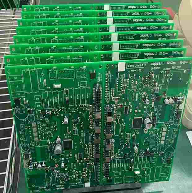
Professional PCB manufacturing and assembly
Building 6, Zone 3, Yuekang Road,Bao'an District, Shenzhen, China
+86-13410863085Mon.-Sat.08:00-20:00


The deformation causes of PCB board processing are very complex and can be divided into thermal stress and mechanical stress.
The thermal stress is mainly produced in the process of pressing, and the mechanical stress is mainly produced in the process of stacking, handling and baking. The following is a brief discussion in process order.
1. Incoming materials of copper clad plate:
Copper clad plates are double panels, symmetrical structure, no graphics, copper foil and glass cloth CTE is almost the same, so in the process of pressing almost no deformation caused by different Ctes.
However, the large size of the copper clad plate press and the temperature difference in different areas of the hot plate will lead to slight differences in the curing speed and degree of the resin in different areas during the pressing process. Meanwhile, the dynamic viscosity under different heating rates is also very different, so the local stress caused by the difference in the curing process will also be generated.
Generally, the stress will maintain balance after pressing, but will gradually release and produce deformation in the future processing.
2. Pressing:
The pressing process of PCB is the main process of generating thermal stress. Similar to the pressing process of copper clad plate, it will also produce local stress caused by the difference of curing process. The thermal stress of PCB board will be more and more difficult to eliminate than that of copper clad plate due to the thicker thickness, diversified pattern distribution, more semi-cured sheets and other reasons.
The stress in the PCB board is released in the process of drilling, shaping or barbecuing, resulting in the deformation of the board.
3. Welding resistance, character and other baking process:
Since the solder resistance inks cannot be stacked on each other when they are solidified, PCB boards will be placed vertically on the shelf for drying board curing. The solder resistance temperature is about 150℃, which is just above the Tg point of medium and low Tg materials. The resin above the Tg point is in high elastic state, and the board is easy to be deformed under the action of dead weight or strong wind of oven.
4. Hot air solder leveling:
The temperature of the tin furnace is 225℃~265℃, and the time is 3S-6S. The temperature of hot air ranges from 280 ° C to 300 ° C.
Solder plate from room temperature into the tin furnace, out of the oven within two minutes and room temperature post-treatment washing. The whole hot-air solder leveling process is sudden heating and sudden cooling process.
Due to the different materials and uneven structure of the circuit board, thermal stress will inevitably occur in the process of cooling and heating, resulting in microscopic strain and overall deformation and warping.
5. Store:
The storage of PCB board in the semi-finished product stage is generally vertically inserted in the shelf, the shelf tightness adjustment is not appropriate, or the stacking of the board in the storage process will cause mechanical deformation of the board. Especially for the thin plate less than 2.0mm, the impact is more serious.
In addition to the above factors, there are many factors affecting PCB board deformation.
PCB board warping deformation prevention
Circuit board warping has a great influence on the production of printed circuit board, and it is also one of the important problems in the process of circuit board manufacturing. The board of components is bent after welding, and the component feet are difficult to be neat.
The board cannot fit into the socket in the case or machine, so the warping of the board will affect the normal operation of the entire post-process.
At present, the printed circuit board has entered the era of surface installation and chip installation. So we need to find out why the circuit board warped.
1. Engineering Design:
Points to note in the design of printed board:
A. The arrangement of semi-cured sheets between layers should be symmetrical, such as six-layer sheets, and the thickness between 1 ~ 2 and 5 ~ 6 layers should be consistent with the number of semi-cured sheets, otherwise it is easy to warp after lamination.
B. Multilayer core plates and semi-cured sheets shall be made from the same supplier.
C. The line graphic area of the outer side A and side B should be as close as possible. If side A is a large copper surface, and side B is only a few wires, the printed board will warpage easily after etching. If the line area difference between the two sides is too large, some independent grids can be added on the sparse side to balance.
2. Drying plate before blanking:
The purpose of drying the copper clad sheet before blanking (150 degrees Celsius, 8±2 hours) is to remove the moisture in the sheet, while fully curing the resin in the sheet, further eliminating the remaining stress in the sheet, which is helpful in preventing the warping of the sheet.
At present, many double-sided, multilayer boards still adhere to the process of drying before or after blanking. However, there are some exceptions for board factories. At present, PCB factories have different time regulations for drying boards, ranging from 4 to 10 hours. It is suggested to decide according to the grade of printed boards produced and customers' requirements for warpage degree.
It is feasible to cut into pieces and bake or whole aniseed after drying. It is recommended to cut the material and bake the board. The inner plate should also be baked.
3. Warp and weft direction of the semi-cured sheet:
The meridional and zonal shrinkage of semi-cured laminates are not the same, so the meridional and zonal shrinkage must be distinguished during blanking and lamination. Otherwise, it is easy to cause warping of the finished plate after lamination, even if the pressure drying plate is difficult to correct.
Many of the reasons for the warping of multilayer plates are caused by the random placement of the warp and weft of the semi-cured sheet when laminating.
How to distinguish longitude and latitude? The direction of the rolled semi-cured sheet is meridional, and the width direction is zonal. For copper foil plate, the long side is zonal, and the short side is meridional. If you are not sure, you can inquire from the manufacturer or supplier.
4. Stress removal after lamination:
After hot and cold pressing, the sheet is removed, the rough edges are cut or milled, and then placed flat in the oven at 150 degrees Celsius for 4 hours to gradually release the stress in the sheet and completely cure the resin. This step cannot be neglected.
5. The plate needs to be straightened when electroplating:
0.4 ~ 0.6mm ultra-thin multilayer plate for plate plating and graphic plating should be made of special clamping roller, in the automatic plating line on the flying bus on the plate, with a round stick to the whole strip of flying bus clamping roller string, so as to straighten all the roller, so that the plate will not be deformed after plating.
Without this measure, the sheet will bend and be difficult to remedy after electroplating a copper layer of 20 or 30 microns.
6. Cooling of the board after hot air leveling:
The hot air of printed circuit board is impacted by the high temperature of the solder groove (about 250 degrees Celsius). After taking out, it should be placed on the flat marble or steel plate for natural cooling, and then sent to the processor for cleaning. It's good for warping the board.
In order to enhance the brightness of the surface of lead tin, some factories put the board into cold water immediately after the hot air leveling, and take it out after a few seconds for post-treatment. This kind of hot and cold impact is likely to produce warping, layering or foaming for some types of board.
In addition, the equipment can be equipped with an air floating bed for cooling.
7. Handling of warping board:
In well-managed factories, printed boards will be checked for 100% smoothness during final inspection. All the unqualified boards will be picked out, put in the oven, 150 degrees Celsius and pressure for 3 to 6 hours, and natural cooling under pressure.
Then remove the board from the pressure relief, and check the flatness again. This can save part of the board. Some boards need to be baked for two or three times before they can be leveled. If the above anti-warping process measures are not implemented, part of the board drying and pressing is useless, can only be scrapped.


Just upload Gerber files, BOM files and design files, and the KINGFORD team will provide a complete quotation within 24h.