
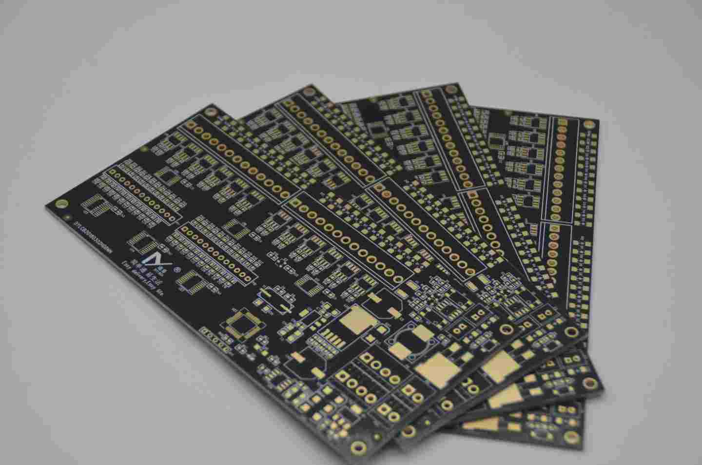
Professional PCB manufacturing and assembly
Building 6, Zone 3, Yuekang Road,Bao'an District, Shenzhen, China
+86-13410863085Mon.-Sat.08:00-20:00

Using Laser photo plotters(laser plotters), they are producing wiring film, solder resistance film, printing film and other films necessary in manufacturing engineering. Wiring film. Film in the paste process, how much there will be a little error, especially for the plate, the error will be a little larger. So in circuit board design to fully consider the impact of these errors, to make a suitable design.
(2) plate cutting manufacturing circuit board board at the factory size is generally 1m×1m or 1m×1.2m. According to the needs of production cut into different sizes of work (work), according to the size of their own design of the PCB circuit board to select the size of the given workpiece, to avoid waste, increase the cost of unnecessary.
(3) Forming of the inner circuit Next, the inner circuit wiring is formed (1-5 in Figure 2). A dry film with light sensitivity is pasted onto a double-sided copper printed circuit board that serves as the inner layer, and then the film used to make the inner layer is exposed, and then the development is carried out, leaving only the place where the wires are needed. The project should be carried out on both sides. The unwanted copper foil should be removed by Etching the device.
(4) Oxygen gasification punishment (blackening punishment) before synthesis with the outer layer, copper foil should undergo oxygen gasification punishment to form a small concave and convex surface. This is to increase the contact area between the semi-curing agent (prepreg), which has insulation and adhesive properties, and the inner layer, so that the adhesion is better. Now in order to reduce environmental pollution, the development of oxygen gasification to punish the product, and now the circuit plate itself has wonderful contact.
(5) Lamination emission punishment Lamination emission punishment, after oxygen gasification emission punishment of the inner circuit, covered with semi-curing agent, and then affixed with the outer copper plate. In vacuum state, while heating, through the laminating machine for compression. The semi-curing agent acts as adhesion and insulation. After the lamination, the appearance looks the same as that of the double-sided copper plate, and the subsequent engineering is the same as that of the double-sided copper plate.
(6) Open hole CNC machine tools for opening operations.
(7) Removal of residue because the heat generated when opening the hole will cause the supplement to dissolve, and adhere to the inner wall of the electroplating hole, can be removed by chemical drugs, make the inner wall smooth and increase the reliability of copper plating.
(8) Copper plating inner and outer layer connection needs to request to take part in copper plating to send punishment, the first is no electrolytic plating, the formation of the minimum thickness of the flow of current. Secondly, in order to achieve the plating thickness required by the design, electrolytic plating is punished. Because the outer copper foil is also attached to the copper plating, the thickness of the outer wire is the thickness of the copper foil plus the plating thickness.
(9) the formation of the outer PCB board and the formation of the inner circuit is the same, affixed with sensitive dry film, and then close to the upper surface wiring film, exposure, exposure phenomenon, leaving only the place where the line needs to go, both sides of the punishment, and then, by etching punishment, do not remove the copper foil.
(10) Making solder stop layer In order to form the pad, it is necessary to carry out solder stop layer (insulation layer) forming punishment, but also to protect the copper foil and better insulation. This can be done by applying the film directly, again using a naturally occurring resin before applying the film, and removing unwanted areas through exposure and development.
(11) Surface release punishment of no solder resistance layer and exposed copper parts, in order to prevent oxygen gasification, need to carry out lead, lead-free copper plating, electrolytic or non-electrolytic gold plating, still water-soluble chemical cleaning agent surface release punishment.
(12) printing ordinary printing is white, welding resistance layer is green. For the LED lamp circuit board, in order to achieve a better effect of strengthening the light source, the printing is black, and the welding resistance layer is white. Still omit printing altogether.
Printing can be used to install and check the numbering of electronic components. But in order to the secrecy of the circuit, there are special circumstances to sacrifice the printed word.
(13) Contour processing through the digital choke punching machine or mold to the circuit board contour punishment
(14) Electrical testing engineering through special electrical testing equipment, circuit breaker and short circuit detection of the circuit board
(15) Shipment can be shipped after checking the appearance and quantity of the circuit board. Generally, deoxygenated gas material is used for packaging, and it is still directly taken to the factory where the components are installed.


Just upload Gerber files, BOM files and design files, and the KINGFORD team will provide a complete quotation within 24h.