
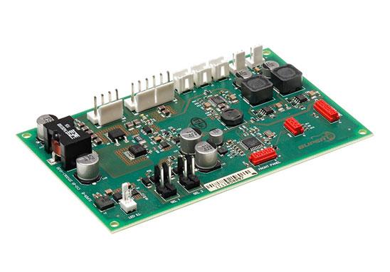
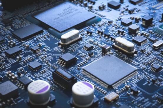
Professional PCB manufacturing and assembly
Building 6, Zone 3, Yuekang Road,Bao'an District, Shenzhen, China
+86-13410863085Mon.-Sat.08:00-20:00

What do the holes in the circuit board do?
It's not exactly a hole. The technical term is a hole. The holes on the circuit board (PCB) are divided into three categories: overcurrent holes (VIA), plug-in holes and installation holes. The hole plays the role of conduction and heat dissipation; The plug-in hole is used for welding components, and the corner of the component is inserted with tin fixed; Mounting holes are used to make screws and can be assembled with other parts.
Generally speaking, the hole and the plug-in hole are metallized holes (PTH), that is, the hole wall is metal attached, can conduct electricity, and the installation hole is generally nonmetallic holes (NPTH), the hole wall is the base material.
This hole is produced by numerical control drilling machine or laser, and then through chemical copper plating, copper plating, surface treatment (common spray tin and gold, other anti-oxidation, tin, etc.).
Generally we see the PCB circuit board has a variety of colors, that is called solder solder ink, prevent short circuit, can also protect the board, play a beautiful role. Welding resistance will also be printed on the above character, easy to identify components during welding maintenance. Ink has green, red, blue, black, white and so on.
The surface of the circuit board is very porous, which is usually divided into the following types:
1, represents the separation of the original installation hole
It is to install in-line (separated) components on the circuit board through certain technological requirements.
2: indicates the heat dissipation hole
This is a kind of heat dissipation hole, and on the other side is a CPU chip.
3, which means through the hole
This hole is used for connecting the front and back wires of the circuit board.
4: indicates the mounting hole
Mounting hole, as the name suggests, is used to install the fixed circuit board.
5. Holes required by other technical specifications
For example, power supply circuit boards, such as transformers, there are some holes or slots in order to ensure the technical performance requirements.
It's called a through hole, if it goes from the top to the bottom, it's called a through hole, if it's in the middle or halfway through, it's called a blind hole. If there is no attribute, that is to say, the hole is not connected to the circuit, it is generally the installation hole or used to match the structure, the hole is generally relatively large, if it is connected to the circuit inside, it is generally connected to two layers of circuit, can be used as a wire, if it is very porous array, is generally used for heat dissipation or to adapt to large current.
What is the round blank pad on the PCB?
The PCB designed by electronic engineers not only needs to realize various functions of the product, but also can realize the automatic production of large modules. In the process of PCBA production, there are steps such as program burning, ICT testing, function testing, etc. After various tests, products delivered to consumers can be guaranteed to be qualified. Program burning and various functional tests require the participation of test points. Some round empty pads on the PCB are the test points. Different factories have different production methods and processes. Some factories will solder the test points, while some factories will not solder the test points.
The test point is actually connected to a network of lines. Such as a test point for program burning, which is connected to the chip's burning pin. For example, in the production process, we need to test the voltage of a certain network. We just need to add a test point to the network and test the voltage of the point through the test equipment. If we add test points to all the networks of PCB, we can test the on and off of each network, so that we can quickly test whether there is a short circuit or open circuit of various components. You can also test to see if the wrong component is attached.
How to test through the test point?
During the production of printed circuit board, the load production test engineer will design the mould for the PCBA test. The welded PCBA will be placed on the test stand, and the test pin on the test stand will be connected to the test point on the PCB board, so that the test can be carried out according to the test requirements. For example, test voltage, current, waveform and so on at each position. If the program is to be burned, the test pin needs to be connected to the corresponding function pin of the burner. The size of the test needle is very small, so the positioning of PCB and the placement of the test needle must be relatively accurate. In order to reduce the difficulty of testing, if the PCB area is allowed, electronic engineers can try to increase the area of test points and the distance between test points when designing PCB.


Just upload Gerber files, BOM files and design files, and the KINGFORD team will provide a complete quotation within 24h.