
Professional PCB manufacturing and assembly
Building 6, Zone 3, Yuekang Road,Bao'an District, Shenzhen, China
+86-13410863085Mon.-Sat.08:00-20:00

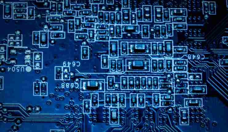
What is impedance
In a circuit with resistance, inductance, and capacitance, the resistance to alternating current is called impedance. Impedance is often represented by Z, is a complex number, the real part is called resistance, the imaginary part is called reactance, where the capacitor in the circuit to AC current obstruction effect is called capacitive reactance, inductance in the circuit to AC current obstruction effect is called inductive reactance, capacitance and inductance in the circuit to AC current caused by obstruction effect is called reactance. The unit of impedance is ohms.
Impedance type
(1) Characteristic impedance
In computer, wireless communication and other electronic information products, PCB line transmission energy, is a square wave signal composed of voltage and time (known as pulse), it encountered resistance is called characteristic impedance.
(2) differential impedance
Two identical signal waveforms of opposite polarity are input at the driving end, which are respectively transmitted by two differential wires. The two differential signals are subtracted at the receiving end. Differential impedance is simply the impedance Zdiff between two lines.
(3) odd-mode impedance
The impedance of one of the two lines to the ground Zoo, the impedance values of the two lines are the same.
(4) even mode impedance
The driving end inputs two identical signal waveforms of the same polarity, and the impedance Zcom when the two lines are connected.
(5) common-mode impedance
The impedance of one line of the two lines to the ground is Zoe, and the impedance values of the two lines are the same, usually larger than the odd-mode impedance.
Why should PCB circuit boards do impedance
pcb circuit board impedance refers to the resistance and reactance of the parameter, the alternating current plays an obstruction role. Impedance processing is essential in pcb circuit board production. Here's why:
1, PCB line (bottom of the board) to consider plug installation of electronic components, plug into the electrical performance and signal transmission performance, so it will require the lower the impedance, the better, resistivity is lower than 1&TImes per square centimeter; Below 10-6.
2, PCB circuit board in the production process to experience copper sinking, electroplating tin (or electroless plating, or hot spray tin), solder joints and other processes, and the materials used in these links must ensure the resistivity bottom, in order to ensure that the overall impedance of the circuit board is low to meet the product quality requirements, can operate normally.
3, the tin plating of PCB circuit board is the most prone to problems in the production of the whole circuit board, is the key link affecting the impedance. The biggest defect of electroless tin layer is easy to change color (easy oxidation or delixing), poor brazing, which will lead to the welding of the circuit board, high impedance leading to poor conductivity or instability of the whole board performance.
4, PCB circuit board in the conductor will have a variety of signal transmission, when to improve its transmission rate and must improve its frequency, the line itself if the etching, laminated thickness, wire width and other factors are different, will cause impedance value change, so that the signal distortion, resulting in circuit board performance decline, so it is necessary to control the impedance value in a certain range.

Impedance for PCB circuit board significance
For the electronic industry, according to the investigation in the industry, the most fatal weakness of the chemical tin layer is easy to discolor (easy oxidation or moisture), poor brazing resulting in difficult welding, impedance is too high leading to poor conductivity or instability of the whole board performance, easy to lead to long tin PCB circuit short circuit and burn or fire events.
It is reported that the first study of chemical tin plating in China is the Kunming University of Science and Technology in the early 1990s, and then Guangzhou Tongqian Chemical (enterprises) in the late 1990s. Until now, the two institutions have been recognized within the industry for 10 years is the best. Among them, according to our contact screening investigation of many enterprises, experimental observation and long-term endurance test, confirmed with the same small chemical tinning layer is a pure tin layer of low resistivity, conductive and brazing quality can be guaranteed to a higher level, no wonder they dare to guarantee its coating without any closed and anti-color agent protection, can maintain a year without discoloration, no foaming, no peeling, forever A tin beard does not grow long.
Later, when the whole social production industry developed to a certain extent, many participants often belong to each other, in fact, quite a number of enterprises themselves did not research and development or initiative ability, so, resulting in a lot of products and users of electronic products (circuit board bottom or electronic products as a whole) performance is poor, and the main reason for poor performance is because of impedance problems , because when unqualified chemical tin plating technology is used, the tin plated for PCB board is not really pure tin (or pure metal elemental), but a tin compound (that is, not a metal elemental at all, but a metal compound, oxide or halide, more directly a non-metallic substance) or a mixture of tin compound and tin gold elemental substance. But it's hard to see with the naked eye... .
Because the main circuit of the PCB circuit board is copper foil, in the solder joint of the copper foil is tin layer, and the electronic components is through the solder paste (or solder line) welding in the tin layer above, in fact, the solder paste in the state of melting welding to the electronic components and tin coating between the metal tin (that is, a good conductive metal), so it can be simply pointed out that the electronic components are through the tin The coating is connected with the copper foil at the bottom of the PCB board, so the purity and impedance of the tin coating is the key; Also, but before inserting electronic components, we directly use the instrument to detect impedance, in fact, both ends of the instrument probe (or pen) is also through the first contact with the copper foil surface at the bottom of the PCB board tin coating and copper foil at the bottom of the PCB board to communicate the current. Therefore, tin coating is the key, is the key to affect the impedance and the key to affect the performance of the entire PCB board, is also easy to be ignored.
As we all know, in addition to the metal elemental, its compounds are electrical conductors or even non-conductive (in addition, this is also the key to the existence of distribution capacity or distribution capacity in the line), so the existence of such conductive but non-conductive tin compounds or mixtures in the tin coating, its ready-made resistivity or future oxidation, moisture after the occurrence of electrolytic reaction resistivity and its corresponding impedance Is quite high (enough to affect the level or signal transmission in a digital circuit) and its characteristic impedance is inconsistent. Therefore, it will affect the performance of the circuit board and its complete machine.
Therefore, in terms of the current social production phenomenon, the coating material and performance on the bottom of PCB board is the most important and direct reason affecting the characteristic impedance of PCB board, but because of its change with the coating aging and moisture electrolysis, so the impact of its impedance becomes more recessive and variable, the main reason for its hidden is: The first can not be seen by the naked eye (including its changes), the second can not be always measured, because it has changes with the change of time and environmental humidity, so it is always easy to be ignored


Just upload Gerber files, BOM files and design files, and the KINGFORD team will provide a complete quotation within 24h.