
Professional PCB manufacturing and assembly
Building 6, Zone 3, Yuekang Road,Bao'an District, Shenzhen, China
+86-13410863085Mon.-Sat.08:00-20:00


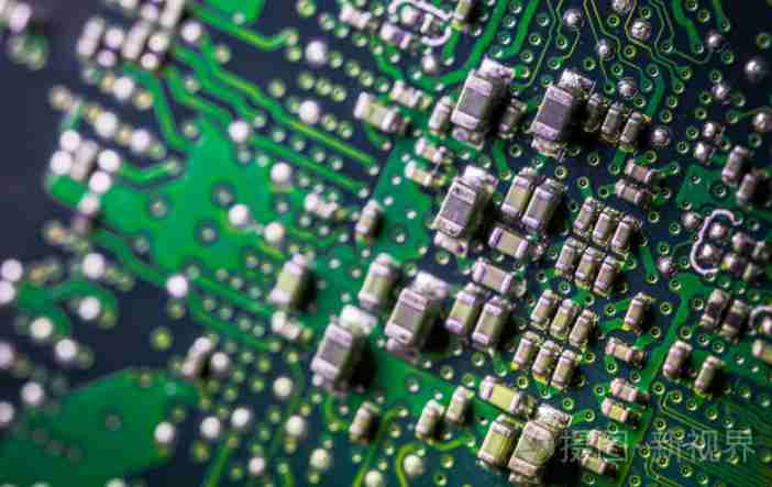
These components cannot be inserted or attached to the holes and surface pads of the circuit board and can even damage automatic cassette loaders. Welded circuit board components, bending components, feet neatly cut.
Circuit boards can't be installed in the case, or in the socket inside the machine, so it's also very annoying for the assembly plant. Current surface mount technology is moving towards high precision,The development of high speed and intelligent direction has put forward higher requirements for the smoothness of PCB board made of various components. PCB board is made of copper foil, resin and glass cloth.
The physical and chemical properties of all materials are different. After pressing, residual thermal stress and deformation will be generated. At the same time, in the process of PCB processing, after high temperature, mechanical cutting, wet processing and other procedures,
Will also have an important impact on plate deformation, PCB board deformation causes are complex, how to reduce or eliminate the deformation caused by the material properties or processing technology is different, has become PCB manufacturing enterprises
One of the most complex problems faced.
2, the deformation of PCB board deformation analysis needs to be from the material, structure, graphic distribution, processing process, etc.
This article will analyze and explain the various reasons for the deformation and improvement methods. The area of copper pavement on the circuit board is not uniform, which will make the bending of the board and the bending of the board worse. General circuit board design will have one
A large area of copper foil as the ground, sometimes Vcc layer can be designed into a large area of copper foil, copper foil can not be uniformly distributed in these large areas at the same time on the circuit board, will cause heating and
Of course, the board will produce thermal expansion and contraction, if the expansion cannot be at the same time, it will lead to different stresses and deformation, if the temperature of the board has reached the limit of Tg value
, the board will begin to soften, causing permanent deformation.
Most PCBS today are multilayer, and there is a connection point between the ribbed pin and the layer (through hole). Connection points can also be divided into through holes, blind holes and buried holes. The position of the connection points will restrict the plate。
The effect of expansion and contraction of the material will also indirectly cause bending and warping of the plate. General return furnace will use a chain on both sides of the chain to drive the circuit board on the return furnace, the board support.
When you build a board, if there's something heavy on the board, or if the size of the board is too big, it will show up because of the dents in the middle.
How to prevent the plate behind the plate bending and plate warping?
Since "temperature" is the main source of stress of the plate, as long as the temperature of the reflux furnace or reduce the heating and cooling rate of the plate in the reflux furnace, the bending of the plate will be greatly reduced.
The occurrence of buckling and plate warping. But there may be other side effects as well. Tg of high Tg plate is the glass transition temperature, that is, the glass transition temperature made of glass material into rubber, and the Tg value of the material.
The lower it is, the faster the softening speed of the plate after entering the reflux furnace, but the longer it takes to become soft rubber, the more serious the deformation of the plate will be. The ability to withstand stress and deformation can be achieved through higher Tg
Plate to increase, but the relative price of materials is also higher.
In order to achieve this goal, the most important way is to improve the production efficiency of the production line. The SMT line consists of a number of equipment, including screen presses, SMT machines, reflow soldering, etc., but in reality, the speed of the line is determined by the SMT machine.

SMT lines are usually composed of high speed and high precision chip patch units, the former mainly mounting components, the latter mainly mounting IC and profiled-shape components.
When two SMT mounters complete an installation (hereinafter referred to as installation time) in equal and minimum time, the full production capacity of the entire SMT line will be brought into full play.
To achieve this, we can handle the load loader as follows. Load the allocated balance. Allocate the number of components for each device to ensure that the installation time for each device is the same. We put the number of parts in the initial paste distribution of each piece of equipment, often with time intervals, which requires that the production load of all the adjusted parts be installed on one piece of equipment according to the installation time of each piece of equipment on the production line. Elements of the same type are arranged together to reduce the number of nozzles used to pick up elements attached to the joint and to save installation time.
Select a large number of feeders should be placed near the printed board. In the up and down cycle, only from the front or back of the material station whenever possible to reduce the head shift distance. Ensure that the mounting head is fully loaded during each cycle. Some principles conflict with the optimization process, so compromise is needed to choose the best optimization solution. Optimization software can be used for load distribution and equipment optimization. The optimization software includes equipment optimization program and production line balancing software. The device optimization program optimizes the placement process and feeder configuration.
In components of BOM and CAD data, it can generate installers and feeder configurations, optimize motion paths and feeder head configuration optimizers to minimize travel heads and thus save assembly time. Production line balancing software is an effective tool for the optimization of the whole production line. The optimization software adopts certain optimization algorithm and has certain intelligence, which can complete the optimization process faster and better. The MTT production line is made up of multiple automated equipment.
When the speed of one equipment is slower than that of other equipment, it will become the bottleneck restricting the speed of the entire SMT line. According to a sample survey of 19 factories, there are frequent bottlenecks in the SMT machines, which can only be eliminated by adding more SMT machines. Of course, this requires a large capital investment, but it can make full use of the remaining capacity of other equipment, which is more cost-effective than purchasing SMT production lines.
Etching process of PCB outer circuit board
Feb 05,2023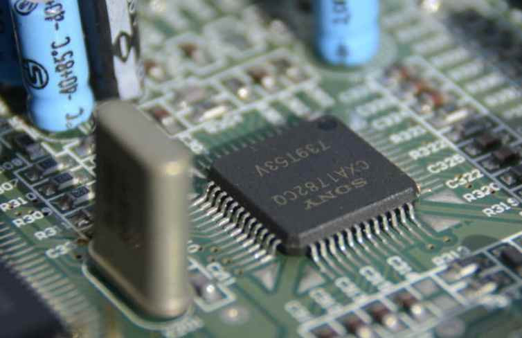


Just upload Gerber files, BOM files and design files, and the KINGFORD team will provide a complete quotation within 24h.