
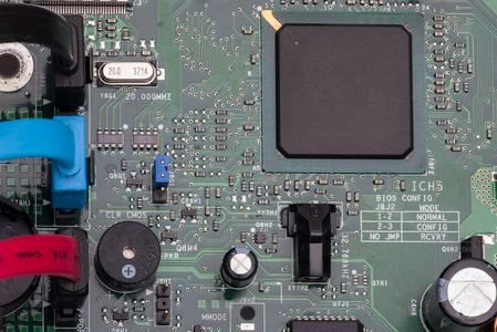
Professional PCB manufacturing and assembly
Building 6, Zone 3, Yuekang Road,Bao'an District, Shenzhen, China
+86-13410863085Mon.-Sat.08:00-20:00

1. Preparation before design
Before the design begins, it is necessary to think and determine the design strategy, so as to guide the selection of components, process selection and cost control of circuit board production. In the case of SI, research should be conducted in advance to form planning or design guidelines to ensure that the design results do not have obvious SI problems, crosstalk or timing issues.
2. Layering of circuit boards
Some project teams have a lot of discretion in how many PCB layers to set, while others don't, so it's important to know where you stand.
Other important questions include: What are the expected manufacturing tolerances? What is the expected insulation constant on the board? What is the allowable error in line width and spacing? What is the allowable error for the thickness and spacing of the grounding and signal layers? All of this information can be used during the pre-wiring phase.
Based on the above data, you can choose to cascade. Note that almost every PCB inserted into another circuit board or backboard has a thickness requirement, and most board manufacturers have fixed thickness requirements for the different types of layers they can make, which will greatly constrain the final number of layers. You may want to work closely with the manufacturer to define cascading numbers. Impedance control tools should be used to generate target impedance ranges for the different layers, making sure to take into account manufacturer-supplied allowable manufacturing errors and the effect of adjacent wiring.
Ideally, when the signal is intact, all high-speed nodes should be wired inside the impedance control layer (e.g. ribbon lines). To optimise the SI and keep the boards decoupled, the grounding/power layers should be arranged in pairs whenever possible. If you can only have one docking layer/power layer, you'll have to make do. If there is no power layer at all, by definition you may run into SI problems. You may also run into situations where it is difficult to emulate or emulate the performance of the board without defining the return path of the signal.
3. Crosstalk and impedance control
Coupling from adjacent signal lines causes crosstalk and changes the impedance of the signal line. Coupling analysis of adjacent parallel signal lines may determine the "safe" or expected spacing (or length of parallel wiring) between signal lines or between various types of signal lines.
For example, if you want to limit the crosstalk from the clock to the data signal node to 100mV, but keep the signal lines parallel, you can find, by calculation or simulation, the minimum allowable distance between the signals on any given wiring layer. Also, if the design includes impedance critical nodes (either clocks or dedicated high-speed memory architectures), you must place the wiring on one (or several) layers to get the desired impedance.

4. Important high-speed nodes
Delay and time delay are the key factors that must be considered in clock routing. Because of the strict timing requirements, such nodes usually have to be terminated to achieve the best SI quality. These nodes are identified in advance and the time required to place and wire the regulating elements is planned to adjust the pointer to the signal integrity design.
5. Technology selection
Different driving techniques are suitable for different tasks. Is the signal point-to-point or point-to-multiple taps? Is the signal coming out of the PCB circuit board or staying on the same PCB circuit board? What is the allowable time delay and noise margin? As a general criterion for signal integrity design, the slower the conversion speed, the better the signal integrity. There is no reason for a 50MHZ clock to have a 500PS rise time. A 2-3NS swing rate control device should be fast enough to ensure SI quality and help solve problems such as output synchronous switching (SSO) and electromagnetic compatibility (EMC).
The advantage of driver technology can be found in new FPGA programmable technology or user-defined ASics. With these custom (or semi-custom) devices, you have a wide range of options for driving range and speed. Early in the design process, meet FPGA (or ASIC) design time requirements and determine appropriate output choices, including pin selection if possible.
In this design phase, appropriate simulation models should be obtained from IC suppliers. In order to effectively cover the SI emulation, you will need an SI emulation program and the corresponding emulation model (possibly the IBIS model).
Finally, you should establish a series of design guidelines during the pre-wiring and wiring phases, which include: target layer impedance, wiring spacing, preferred device processes, critical node topology, and terminal planning.
6. Pre-wiring stage
The basic process of pre-wiring SI planning is to first define input parameter ranges (drive amplitude, impedance, tracking speed) and possible topological ranges (minimum/maximum length, short line length, etc.), then run each possible simulation combination, analyze timing and SI simulation results, and finally find an acceptable numerical range.
Next, the working range is interpreted as the wiring constraints of PCB wiring. Different software tools can be used to perform this type of "sweep" preparation, and the wiring program automatically handles such wiring constraints. For most users, timing information is actually more important than SI results, and the results of interconnection simulation can change the wiring to adjust the timing of the signal path.
In other applications, this process can be used to determine the layout of pins or devices that are incompatible with system timing Pointers. At this point, it is possible to fully determine which nodes need to be wired manually or which do not need to be terminated. For programmable devices and ASics, the choice of output drivers can also be adjusted at this time to improve the SI design or avoid discrete terminating devices.
7. SI simulation after wiring
In general, it is difficult for SI design guidelines to ensure that no SI or timing problems will occur after the actual wiring is completed. Even if the design is guided by guidelines, unless you can continuously check the design automatically, there is no guarantee that the design will fully comply with the guidelines, and problems will inevitably arise.
Post-wiring SI emulation checks will allow design rules to be systematically broken (or changed), but only as necessary for cost reasons or strict wiring requirements.
8. Post-manufacturing stage
The above measures can ensure the SI design quality of the circuit board. After the circuit board assembly is completed, it is still necessary to put the circuit board on the test platform, measure it with oscilloscope or TDR (time domain reflectometer), and compare the real circuit board with the simulation expected results. These measurements can help you improve the model and manufacturing parameters so that you can make better (and less constrained) decisions on your next pre-design survey.
9. Selection of model
Much has been written about model selection, and engineers doing static timing validation may have noticed that, despite all the data available from device data sheets, it is still difficult to build a model. SI simulation model is on the contrary, it is easy to build the model, but it is difficult to obtain the model data. In essence, the only reliable source of SI model data is the IC vendor, who must work in tacit coordination with the design engineer.
The IBIS model standard provides a consistent data carrier, but the cost of building the IBIS model and ensuring its quality is high. IC vendors still need to invest in it to be demand-driven, and circuit board manufacturers may be the only demand-side market.
PCB design to ensure signal integrity
By summarizing the factors that affect the signal integrity, we can better ensure the signal integrity in the PCB design process from the following aspects.
(1) Circuit design considerations. Including controlling the output number of synchronous switching, controlling the maximum edge rate of each unit (dI/dt and dV/dt), so as to obtain the lowest acceptable edge rate; Select differential signals for high output functional blocks such as clock drivers; Passive components (such as resistors and capacitors) are connected at the upper end of the transmission line to achieve impedance matching between the transmission line and the load.
(2) Minimize the length of parallel wiring.
(3) Components should be placed far away from the I/O interconnect interface and other areas susceptible to interference and coupling, and minimize the spacing between components.
(4) Shorten the distance between signal routing and reference plane.
(5) Reduce wire impedance and signal driving level.
(6) Terminal matching. A terminal matching circuit or matching element can be added.
(7) Avoid parallel wiring to provide sufficient spacing between wires and reduce inductive coupling.
Nine steps to PCB signal integrity
Feb 04,2023


Just upload Gerber files, BOM files and design files, and the KINGFORD team will provide a complete quotation within 24h.