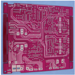
1、 Impact of PCB size design on cost
The size of the original size copper clad plate is too large, which makes PCB processing inconvenient, and sometimes it can not even be put into the PCB processing equipment for processing. Therefore, it is necessary to first cut it into several copper clad plates of processing size. As for the specific size of processing size, it needs to be determined according to the processing equipment for making printed circuit boards, the size of each printed circuit board and some PCB process parameters. In addition to the length and width required by the printed circuit pattern itself, these process parameters also include the width consumed by the screw holes for fixing the printed circuit board to the PCB product frame, the process allowance for contour processing, the fixture clamping allowance for chemical plating, electroplating and corrosion, the positioning pin allowance for multi-layer printed circuit board, the allowance for the alignment marks between layers, the allowance for the marks of the printed circuit board manufacturer, the edge width of the printed circuit board, etc, The recommended values of some process parameters can be obtained from the copper clad plate manufacturers or dealers. During the production and processing of printed circuit, it can be determined according to the above data how many copper-clad boards of processing size are cut from a large original size, whether they are cut longitudinally or transversely, whether they can be nested, etc.

2、 Influence of the number of layers of printed circuit board on cost
With the increase of the number of layers of printed circuit board, the production cost will increase sharply, so it is possible to cause a large difference in cost due to a wrong idea. If you encounter difficulties in designing a 6-layer printed circuit board, you must not give up easily. Maybe a large amount of economic benefits are in your efforts to persist; However, it is not easy to be reluctant, because in most cases, the designer may not hesitate to design an 8-layer printed circuit.
3、 CEM-3 Materials
In addition to the widely used double-sided epoxy resin glass cloth copper clad plate, the double-sided copper clad plate used for making double-sided printed circuit boards also has a low-cost CEM-3 material. Its structure is to change the thicker epoxy resin glass cloth as the base material in the original double-sided epoxy resin glass cloth copper clad plate into two very thin sheets. At this time, due to insufficient strength, The epoxy resin glass non-woven fabric is sandwiched between two thin epoxy resin glass fabrics, thereby reducing the cost. CEM-3 material is soft and can be used as the core material of multi-layer rigid printed circuit board in addition to being used alone.
4、 Effect of the ratio of wire width to gap width of conductor pattern on cost
If the width of the conductive pattern in the printed circuit board is expressed in L and the gap width between the conductive patterns is expressed in S, LIS represents the ratio of the width of the conductive strip to the gap width. With the decrease of this ratio, the production yield of printed circuit board will decrease sharply, and the cost will also rise. This phenomenon is more obvious when the circuit density is relatively high. Therefore, the LIS value must not be arbitrarily reduced.
5、 Impact of through-hole diameter on cost
When a drill bit is used to drill a printed circuit board, when the hole diameter is lower than a certain value, the drilling depth of the drill bit will be sharply shortened. That is to say, when drilling a hole with a small diameter, the drill bit needs to exit the heat dissipation for many times, which will reduce the production efficiency and increase the cost. Therefore, do not arbitrarily reduce the diameter of the through hole; The number of through holes should also be reduced as much as possible.
6、 Fill the through hole with silver paste
For the through hole of double-sided printed circuit board, instead of copper plating, the method of filling silver paste into the through hole can also reduce the cost of double-sided printed circuit board. This method is generally used for ordinary phenolic resin paperboard coated with copper on both sides. The method first cleans the surface of the ordinary phenolic resin paperboard coated with copper on both sides, then prints corrosion resistant graphics on both sides with screen printing method, forms conductor graphics after corrosion, punches through holes after removing the corrosion resistant layer, and then fills the holes with silver paste. In order to make the silver paste be in good contact with the conductor patterns on both sides, the silver paste should be bulged out of the through hole, and the diameter of the silver paste pattern on the bulged part is larger than the hole diameter of the through hole. In order to prevent the migration of silver ions, a covering layer is covered on the surface of the bulged part of the silver paste by screen printing. Then, solder mask graphics and isolation graphics are printed on both sides of the screen, and screw holes for fixing the printed circuit board are punched or drilled to process the shape. Finally, through inspection, the double-sided printed circuit board filled with silver paste through the hole was completed.


