
Professional PCB manufacturing and assembly
Building 6, Zone 3, Yuekang Road,Bao'an District, Shenzhen, China
+86-13410863085Mon.-Sat.08:00-20:00

Differences between Whole Plate Plating and Pattern Plating of High Frequency Plate
PCB manufacturers, PCB designers and PCBA processors will explain the difference between whole board electroplating and graphic electroplating of high-frequency board proofing manufacturers
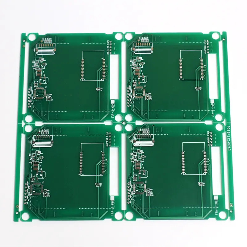
High frequency circuit board is a special circuit board with high electromagnetic frequency. Generally speaking, high frequency can be defined as the frequency above 1GHz. Its physical performance, accuracy and technical parameters are very high, and are commonly used in automotive anti-collision systems, satellite systems, radio systems and other fields.
High frequency plate proofing manufacturers attach great importance to technical problems and strict requirements for each process. Electroplating is also an important process in our high frequency plate production. Now let's talk about the difference between whole plate electroplating and graphic electroplating!
a. The only difference between copper plated whole plate electroplating and pattern electroplating is copper plating. In the whole plate electroplating, the high-frequency plate proofing manufacturer has completely plated the copper before the graphic transfer process. In graphic electroplating, most copper coatings are plated after graphic transfer.
The pattern electroplating method has obvious influence on the size of the pattern. The wire and pad width on each side is generally increased by about the thickness of the coating, that is, if the thickness of the surface coating is 0.001 inch, the wire width will be increased by about 0.002 inch.
High frequency board proofing manufacturer has strict tolerance on high-density printed circuit, so the allowable increased thickness of conductor shall be taken into account when conducting base drawing wiring. Because there is no corrosion inhibitor in the copper electroplating stage of the whole plate, the contamination problem caused by the organic corrosion inhibitor can be eliminated.
In the graphic electroplating of high-frequency board proofing manufacturers, the problem that the high current density area of the insulation part is easy to make the circuit board "scorch" does not exist in the whole board electroplating. However, pattern electroplating requires only a few processes, with low power consumption, and copper consumption is actually reduced. However, the current density must be carefully controlled, especially when the density distribution in the pattern area is uneven.
b. In the whole plate electroplating, a large part of the copper plating must be etched off. In the typical operation of using 1oz copper clad laminate and plating copper in the hole to 0.0015 inch thick, the etching workload will be doubled, so that the consumption of etchant, etching time and wastewater treatment capacity will be doubled, and the unacceptable side erosion phenomenon will be greatly increased. In order to reduce the side corrosion effect in the whole plate electroplating, sometimes a thicker metal corrosion resistant deposit layer is used, which helps to seal the coating edge during etching to a certain extent.
From the above, it can be clearly seen that the main defect of the whole plate electroplating in the high-frequency plate proofing manufacturer is that a lot of etching is required. The use of 1 | 2 oz copper foil copper clad laminate or even thinner copper foil copper clad laminate can reduce the etching problem.
PCB manufacturers, PCB designers and PCBA processors will explain the differences between the whole board electroplating and graphic electroplating of high-frequency board proofing manufacturers.


Just upload Gerber files, BOM files and design files, and the KINGFORD team will provide a complete quotation within 24h.