
Professional PCB manufacturing and assembly
Building 6, Zone 3, Yuekang Road,Bao'an District, Shenzhen, China
+86-13410863085Mon.-Sat.08:00-20:00

The analysis and design of power supply system (PDS) is becoming more and more important in the field of high-speed circuit design, especially in the computer, semiconductor, communication, network and consumer PCB industries. With the inevitable further scaling down of VLSI technology, the supply voltage of integrated circuits will continue to decrease. As more and more manufacturers switch from 130nm technology to 90nm technology, it can be predicted that the power supply voltage will drop to 1.2V or even lower, while the current will also increase significantly. From DC IR voltage drop to AC dynamic voltage fluctuation control, the allowable noise range is getting smaller and smaller, which brings great challenges to the design of power supply system.
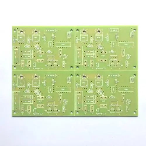
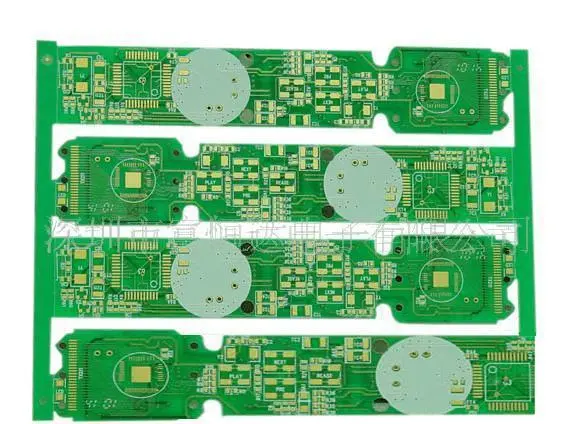
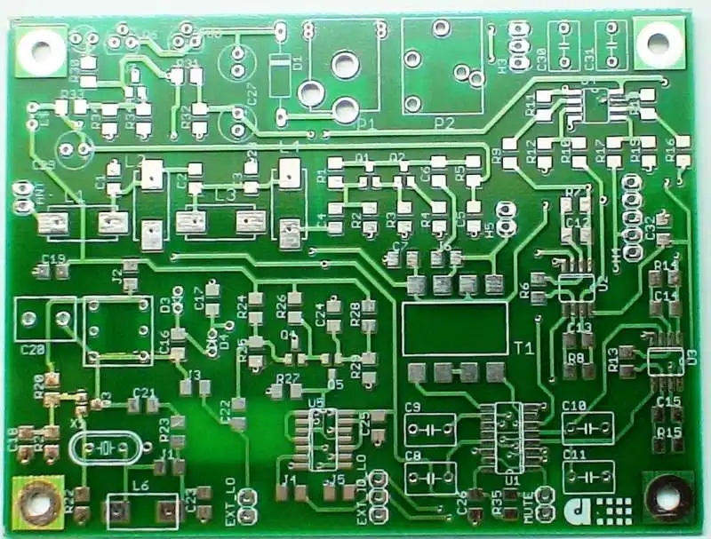
Power pcb design
In AC analysis, the input impedance between power supply and ground is an important measurement to measure the characteristics of power supply system. The determination of this observation becomes the calculation of IR voltage drop in DC analysis. Whether in the analysis of DC or AC, the factors that affect the characteristics of the power supply system are: the layering of PCB, the shape of the power board plane, the layout of components, the distribution of vias and pins, and so on.
The concept of input impedance between power supply and ground can be applied to the simulation and analysis of the above factors. For example, a very wide application of power ground input impedance is to evaluate the placement of on-board coupling capacitors. As a certain number of decoupling capacitors are placed on the board, the unique resonance of the circuit board can be suppressed, thus reducing the generation of noise, and also reducing the edge radiation of the circuit board to alleviate the electromagnetic compatibility problem. In order to improve the reliability of the power supply system and the manufacturing cost of the degraded system, system PCB design engineers must often consider how to economically and effectively select the PCB layout of the system with decoupling capacitors.
The power supply system in high-speed circuit system can generally be divided into three physical subsystems: chip, integrated circuit package structure and PCB. The power grid on the chip is composed of several layers of metal layers placed alternately. Each layer of metal is composed of a power grid or a ground grid of metal strips in the X or Y direction. The vias connect the metal strips of different layers.
For some high-performance chips, the power supply of both the core and IO is integrated with many decoupling units. The integrated circuit packaging structure is like a reduced power supply or ground plane with several layers of complex shape. On the upper surface of the package structure, the mounting position of the decoupling capacitor is usually reserved. PCB usually contains continuous power supply and ground plane with large area, as well as some large and small discrete decoupling capacitor components, and power rectifier module (VRM). Bonding line, C4 bump and solder ball connect the chip, package and PCB together. The whole power supply system should ensure to provide the integrated pcb devices with stable voltage within the normal range. However, switching currents and the parasitic high-frequency effects in power supply systems always introduce voltage noise.


Just upload Gerber files, BOM files and design files, and the KINGFORD team will provide a complete quotation within 24h.