
Professional PCB manufacturing and assembly
Building 6, Zone 3, Yuekang Road,Bao'an District, Shenzhen, China
+86-13410863085Mon.-Sat.08:00-20:00

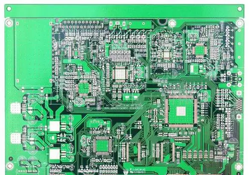
During PCB processing, some PCB engineers do not want to lay copper on the whole board on the surface and bottom to save time. Is this the right thing to do? Is it necessary for PCB to lay copper on the surface and bottom?
First of all, we need to make it clear that it is beneficial and necessary for PCB to lay copper on the surface and bottom, but some conditions must be observed for laying copper on the whole board.
Benefits of Copper Laying on the Surface and Bottom
1. From the EMC point of view, the whole board of the surface and bottom layer is paved with copper, which provides additional shielding protection and noise suppression for the inner signal and the inner signal, as well as some shielding protection for the devices and signals at the surface and bottom layer.
2. From the perspective of heat dissipation, as the current PCB board is becoming more and more high-density, BGA master chip also needs to consider the thermal problem more and more. The whole board flooring copper improves the heat dissipation capacity of PCB board.
3. From the perspective of process, the whole board is paved with copper, which makes the PCB board evenly distributed. The bending and warping of the board are avoided during pressing, and the warping and deformation of the PCB due to different stresses caused by over reflow soldering due to uneven copper foil are avoided.
Reminder: Copper coating is necessary for two-layer boards
On the one hand, since there is no complete reference plane for two layers of PCB boards, the flooring can provide a return path and can also be used as a coplanar reference to achieve impedance control. We can generally use the bottom floor to lay the ground plane, and the top floor to put the main devices and take the power and signal lines. For high impedance circuits, analog circuits (analog digital conversion circuits, switching mode power conversion circuits), copper coating is a good practice
Conditions for surface and bottom copper coating
Although it is good for PCB to lay copper on the surface and bottom, some conditions should be followed:
1. At the same time, try to pave by hand instead of one time to avoid broken copper skin. Properly add vias in the copper paving area to the ground level.
Cause: The copper clad plane on the surface layer must be separated and broken by the PCB components and signal lines on the surface layer. If there is copper foil with poor grounding (especially thin and long copper scrap), it will become an antenna, causing EMI problems.
2. In particular, consider the thermal balance of small devices, such as 0402 0603 and other small packages, to avoid the monument effect.
Cause: If the whole board is covered with copper for full connection of component pins, the heat loss will be too fast, resulting in difficulty in desoldering and repair welding.
3. The whole board flooring should be continuous, and the distance from the flooring to the signal should be controlled to avoid discontinuous transmission line impedance.
Cause: The copper sheet too close to the ground will change the impedance of the microstrip transmission line, and the discontinuous copper sheet will also cause a negative impact on the impedance discontinuity of the transmission line.
4. Some special cases depend on the application scenario. PCB design should not be an absolute design, but should be weighed and applied in combination with the theories of all parties.
Cause: In addition to the need to wrap sensitive signals, if there are many high-speed signal lines and PCB components, many small and long copper scraps will be generated, and the PCB wiring channel is tight, it is necessary to try to avoid the connection between the surface copper sheet and the ground plane through holes. At this time, the surface layer can choose not to lay copper.


Just upload Gerber files, BOM files and design files, and the KINGFORD team will provide a complete quotation within 24h.