

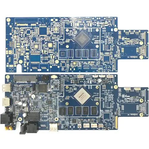
Communication module BGA assembly
Name: Communication module BGA assembly
Number of SMT lines: 7 high-speed SMT patch supporting production lines
SMT daily production capacity: more than 20 million points
Testing Equipment: X-RAY Tester, First Piece Tester, AOI Automatic Optical Tester, ICT Tester, BGA Rework Station
Placement speed: CHIP component placement speed (at best conditions) 0.036 S/piece
The smallest package that can be attached: 0201, the accuracy can reach ±0.04mm
Minimum device accuracy: PLCC, QFP, BGA, CSP and other devices can be mounted, and the pin spacing can reach ±0.04mm
IC type patch accuracy: it has a high level for mounting ultra-thin PCB boards, flexible PCB boards, gold fingers, etc. Can be mounted/inserted/mixed TFT display driver board, mobile phone motherboard, battery protection circuit and other difficult products
Due to the particularity of the BGA packaging form, its rework requires special rework tools, and the rework is difficult and the success rate is low.
For electronic assembly manufacturers, improving the quality of BGA assembly is of great significance for improving product quality and reducing costs.
①Package form of BGA
The current BGA package is mainly divided into PBGA (plastic-packaged BGA), and CBGA (ceramic package) according to the type of substrate.
(packaged BGA) and TBGA (tape-carrier packaged BGA). The PBGA package consists of chips mounted and interconnected to a double-sided or multilayer PCB substrate, with vias interconnecting signal traces on the top surface to corresponding pads on the bottom of the substrate. After chip bonding and wire bonding, the assembled part is molded and encapsulated by transfer molding or injection molding. It is currently the most widely used BGA device, mainly used in communication products and consumer products. Because of its following advantages, it is widely used in SMT assembly: high ratio of I/O terminals to package area: it matches the thermal expansion coefficient CTE of epoxy resin PCB, and has good thermal comprehensive performance:
Good electrical performance; high interconnection density; lower solder ball coplanarity requirements in SMT assembly, generally 0.15~0.20 mm; self-centering function in SMT reflow engineering: eliminates narrow pitch solder paste printing; reduces the possibility of bridging between pads.
PBGA device is a highly humidity-sensitive device, which must be stored under constant temperature and dry conditions to avoid components affected before assembly. Generally, the ideal storage environment for BGA is 20- 25C, and the RH is less than 10% (it is better to have nitrogen protection measures). Therefore, once the BGA-sealed moisture-proof package is opened, it must be assembled on the PCB within the specified time. The period of time that a PBGA chip must be used after unpacking is determined by the sensitivity level of the chip.
During the assembly process, the package of the BGA cannot be assembled within the corresponding time after being opened, and the exposure time exceeds
In order to make the BGA have good solderability before the next use, it is recommended to bake the BGA. The baking temperature should generally not exceed 125°C, and the RH should be lower than 60%, because an excessively high temperature will increase the thickness of the intermetallic compound at the joint between the solder ball and the BGA, and cracks will easily occur during the assembly process, resulting in BGA assembly failure. Baking time is closely related to the moisture sensitivity level of BGA and the thickness of BGA.
PBGA solder ball components are generally Sn63Pb37, Sn62Pb36Ag2 and Sn96.5Ag3. 0Cu0. 5 alloys, solder balls
The spacing is generally 1.50, 1.27, 1.0, 0.8, and 0.5mIn, and the diameter of the solder ball can be adjusted according to different applications.
The required difference varies between 0.75 - 0.30 mIn. For a BGA with a smaller pitch, the higher the packaging density, the higher the process requirements for BGA assembly. The interconnection of CBGA is completed by Snl0Pb90 high-temperature solder balls and soldering the solder balls to the substrate through low melting point solders such as Sn63Pb37, Sn62Pb36Ag2, and Sn96.5Ag3. 0Cu0.5. The diameter of the solder balls used when the pitch of the solder ball array is 1.27 min is 0.89 min, and the diameter of the solder balls used when the pitch is 1.0mm is 0.64 rn/n. The main advantages of CBGA packaging include (1) High reliability and excellent performance of packaged components: (2) Good coplanarity and easy soldering; (3) Insensitive to moisture and long storage time; (4) Good electrical performance : (5) High packing density. The main disadvantage of CBGA is that it does not match the thermal expansion coefficient CTE of the PCB, which can easily cause thermal fatigue failure, so the thermal reliability is poor, and it is difficult to align the edge of the package with the PCB pad, and the packaging cost is high.
TBGA is a packaging form that uses copper/polyimide carrier tape as the substrate to realize the connection between the chip and the solder ball and the PCB.
The TBGA package has the following characteristics: (1) Good thermal matching with the epoxy resin circuit board: (2) Can be aligned with the PCB pad through the edge of the package; (3) Sensitive to humidity and heat, multi-component polymerization of different materials adversely affect reliability.
Due to the particularity of the BGA package, its solder joints are located in the area array structure of the lower part of the BGA package body, and slight deformation of the PCB during the assembly process may cause the open circuit of the BGA solder balls. Therefore, the position design of BGA should be away from areas with large deflection and high-stress areas of PCB, such as the four corners of the PCB, edge positions, connectors, mounting holes, slots, cutting boards, gaps, and corners.
Due to the large heat capacity of BGA, in order to ensure the thermal uniformity of PCB surface components, no components should be placed in the area of 5min around the BGA to avoid deformation due to uneven temperature distribution during PCB assembly.
In order to reduce the deformation of PCB and improve the quality of BGA assembly, good PCB material is needed, especially for the soldering process suitable for lead-free electronic assembly, due to the increase of reflow temperature, higher requirements are put forward for PCB material. The widely used modified FR4 type substrate at present has a value greater than 170°C, which can basically meet the requirements of lead-free and tin-lead reflow soldering processes.
The pad design of the PCB corresponding to the BGA is generally 20% smaller than the diameter of the solder ball, and the pad corresponding to each solder ball should be solid copper
The maximum diameter of the PCB pad is the pad diameter of the solder ball at the bottom of the BGA device, and the minimum diameter should be the diameter of the bottom pad of the BGA device minus the mounting accuracy. A solder mask should be designed around the pad, and the size of the solder mask should be 0.1 ~ 0.15 mIn larger than the pad to prevent the loss of solder and causing a short circuit or virtual soldering. A through hole should be designed next to the pad. After hole plating, the through hole must be blocked with a dielectric material or conductive glue, and the height must not exceed the height of the pad.
③BGA assembly process
In the BGA assembly process, every step and every process parameter will affect the BGA assembly, so every step of the BGA assembly must be strictly controlled. For tin-lead and lead-free electronic assembly processes, there is not much difference between solder paste printing and chip placement process. The main difference lies in the setting of the temperature curve in the reflow process. There are large differences in welding processes. In addition, due to the different packaging forms of BGA, there are different thermal resistances. In order to meet the requirements of the reflow soldering temperature curve, there are also certain differences in the temperature setting and time.
3.1 Solder paste printing
Solder paste is a uniform mixture of alloy solder powder, flux system, and thixotropic agent system, and has a paste flow with thixotropic properties.
The storage conditions of bulk solder paste are generally stored at 2~5°C for 3-6 months. There will be no chemical changes during storage, there will be no separation of solder powder and flux, and its viscosity and viscosity will remain unchanged. The solder paste must be warmed up naturally before printing, and the general warming time is 4-8 hours. Before the solder paste is warmed to room temperature, do not disassemble the container or stir the solder paste and force it to heat up to avoid damage to the soldering flux. Analysis of the. To ensure good printability and solderability.
The amount of solder paste printing should be appropriate. Too many soldering defects such as bridging may easily occur, and too little solder paste may easily cause soldering defects such as open circuits or virtual soldering.
Pick up defects. The control of solder paste EO, ~U amount depends on the thickness of the printing template, the pressure of the squeegee and the printing speed. The printing template is generally made of stainless steel. The opening diameter of the BGA template is generally slightly smaller than the diameter of the pad, and its thickness is generally 0.12-0.15mm to ensure an appropriate amount of solder paste printing.
When printing solder paste, generally use 60. In stainless steel scraper, the scraper pressure is generally controlled at 35~100 N, the pressure is too small to make
An insufficient amount of solder paste transfer, too large will make the printed solder paste too thin, increasing the possibility of solder paste contamination on the reverse side of the template and the PCB substrate.
The printing speed is generally 10 -25 mllfS. If it is too fast, it will easily cause the scraper to slide and miss printing. If it is too slow, it will easily cause uneven edges of the solder paste imprint and pollute the surface of the PCB substrate. The smaller the pitch of BGA solder joints, the slower the printing speed can ensure good printing quality. The molding speed after printing is generally set at 0. 5~1. 0 mllfS, the smaller the solder joint spacing, the slower the demoulding speed should be. At present, studies have shown that setting the demoulding speed to be accelerated, that is, gradually accelerating from zero, can avoid solder paste collapse and poor separation of solder paste and template during constant speed demoulding, and the demoulding effect is good.
In addition, when printing, pay attention to controlling the operating environment, the temperature is controlled at about 25"C, and the humidity is controlled at about RH55%.
Right, the printed PCB should be reflowed within 30 minutes to prevent the solder paste from being exposed to the air for too long and affecting the assembly quality.
3.2 Patch
The main purpose of patching is to align each solder ball on the BGA with each corresponding pad on the PCB. Since the solder balls on the BGA are located at the bottom of its package, special equipment must be used for alignment. The placement accuracy of the placement machine for placing BGAs must reach about 0.001 rain. BGA devices can be accurately placed on the PCB through image recognition. Because there is a certain deviation in the coplanarity of BGA solder balls and certain differences in solder paste printing, in order to ensure good soldering quality, generally subtract 25-41-50.80 pm from the BGA height, and use the delay to turn off the vacuum system at the same time About 400 ms, so that the solder balls of the BGA can fully contact with the solder paste when mounting, so as to avoid the phenomenon of a certain soldering circuit open circuit of the BGA during the reflow process.
3.3 Reflow soldering
Reflow soldering is a process that is difficult to control in the BGA assembly process. Set process parameters and obtain a suitable temperature curve for
Good soldering of BGA is very important. Due to the different packaging forms of BGA, the thermal resistance of CBGA is larger than that of PBGA, so to achieve the same temperature, CBGA needs a higher temperature setting and longer preheating time than PBGA. For tin-lead solder paste and lead-free solder paste, the temperature setting and heating time are significantly different.
Preheating stage: The main purpose of preheating is to heat the PCB and its components evenly and at the same time have a baking effect on the PCB and components.
The function of baking is to remove the moisture in it and evaporate the appropriate amount of flux in the solder paste. The temperature rise rate in the preheating stage should not be too fast, so as to prevent the PCB from being heated too fast and causing large deformation. - Generally, the heating rate is controlled at 3"C/s, and the preheating time is between 60-90 s.
Activation stage: The main purpose of this stage is to activate the flux in the solder paste, remove the oxides on the surface of the pad and the surface of the solder paste alloy, and achieve a clean metal surface to prepare for the solder paste reflow process. At the same time, the excessive flux in the solder paste is evaporated and the PCB is preheated to prevent the deformation of the PCB caused by excessive temperature rise during the reflow process. For tin-lead soldering, the temperature at this stage should be maintained at 150-180"C for 60-120 S; for lead-free soldering, the temperature at this stage should be maintained at 160-200"C for 60-180 S, so that the flux can fully exert its effect. The temperature rise rate in the activation stage is generally controlled at 0.3 plus .5°C/S.
Reflow stage: At this stage, the temperature of the solder joint has risen above the melting point of the solder paste, and the solder paste is in a molten state. back
The main purpose of the flow stage is to make the molten solder wet the pad and the lead of the component to achieve good soldering requirements. For PBGA, its solder balls are Sn63Pb37, Sn62Pb36Ag2 and Sn96. During the reflow process, the solder balls are not melted, and the solder paste melts and wets the pads and high-temperature solder balls to form solder joints. Therefore, an appropriate time is required to ensure that the molten solder paste can wet the pad and solder ball well. If the time is too short, it may cause poor wetting and form a virtual joint. If the time is too long, a thick gap may be formed between the solder and the pad. - Layer intermetallic compounds Cu6sn5 and Cu3Sn, due to their brittle characteristics, are easy to form cracks and cause solder joint failure. Especially for lead-free electronic assembly, due to the high content of alloying element Sn in lead-free solder, it is easier to form thicker intermetallic compounds at high temperatures, resulting in the failure of solder joints. The time is controlled within 60. -90 s, and the time within the peak temperature range of 210-225"C is controlled within 10-20 s; for lead-free soldering, it is generally required to control the time above the melting point of 217-219C within 60-120 s, among which It is better to control the time in the peak temperature range of 230~235" C within 20~40 s.
Cooling stage: After the solder paste is reflowed, the flux is completely consumed, forming a molten metal solder joint. main cooling phase
The main purpose is to refine the grains while solidifying the solder joints, inhibit the growth of intermetallic compounds, and improve the strength of the solder joints. However, due to the excessive cooling rate, will cause the deformation of PCB and the thermal cracking of electronic components, especially components with large heat absorption such as BGA. If the cooling rate is too fast, it will easily cause damage to the internal package, resulting in the failure of BGA. Generally, the cooling rate is controlled within 1~3C/s.
4. Conclusion
The assembly of BGA is a very complicated process. From the packaging form of BGA, the design of PCB, the characteristics of solder paste and its printing process, the SMT process, and suitable reflow soldering temperature curve, any problem in any process may cause the Failure of BGA assembly. Therefore, in the BGA assembly process, the assembly process must be strictly controlled to improve the assembly quality of the BGA.

Name: Communication module BGA assembly
Number of SMT lines: 7 high-speed SMT patch supporting production lines
SMT daily production capacity: more than 20 million points
Testing Equipment: X-RAY Tester, First Piece Tester, AOI Automatic Optical Tester, ICT Tester, BGA Rework Station
Placement speed: CHIP component placement speed (at best conditions) 0.036 S/piece
The smallest package that can be attached: 0201, the accuracy can reach ±0.04mm
Minimum device accuracy: PLCC, QFP, BGA, CSP and other devices can be mounted, and the pin spacing can reach ±0.04mm
IC type patch accuracy: it has a high level for mounting ultra-thin PCB boards, flexible PCB boards, gold fingers, etc. Can be mounted/inserted/mixed TFT display driver board, mobile phone motherboard, battery protection circuit and other difficult products
