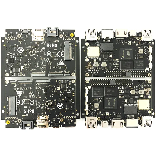
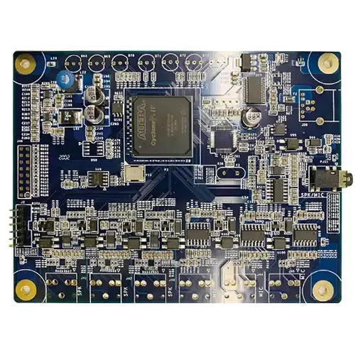
Industrial control board BGA assembly
Name: Industrial control board BGA assembly
Number of SMT lines: 7 high-speed SMT patch supporting production lines
SMT daily production capacity: more than 20 million points
Testing Equipment: X-RAY Tester, First Piece Tester, AOI Automatic Optical Tester, ICT Tester, BGA Rework Station
Placement speed: CHIP component placement speed (at best conditions) 0.036 S/piece
The smallest package that can be attached: 0201, the accuracy can reach ±0.04mm
Minimum device accuracy: PLCC, QFP, BGA, CSP and other devices can be mounted, and the pin spacing can reach ±0.04mm
IC type patch accuracy: it has a high level for mounting ultra-thin PCB boards, flexible PCB boards, gold fingers, etc. Can be mounted/inserted/mixed TFT display driver board, mobile phone motherboard, battery protection circuit and other difficult products
(1) In the BGA assembly work, it is also very important to require a high viscosity of the flux used for SMT patching. If it is too high, it will affect the coating and transfer; if it is too low, it will affect the amount of coating. Generally, the viscosity should be selected in the range of (25000±5000)cp.
(2) The thickness of the flux is 60% of the solder ball. If it is too thick, it is easy to be coated on the package body, causing vibration during soldering, and even optical centering recognition.
(3) Detection method. Generally, a sawtooth ruler can be used to detect, but the height of the sawtooth ruler will be different from the actual BGA chip solder ball due to factors such as sampling position, operation method (immersion speed, time), and sawtooth size.
The glass should be used for observation. A good flux height should obtain a uniform flux pattern under the glass plate, and the size should be at least larger than the solder ball. The device that rotates and scrapes the flux, often the amount of flux obtained is different due to the difference in viscosity. X-rays were used to observe the size of the solder joints, and it was found that the thicker the flux, the larger the diameter of the solder joints, indicating that the amount of solder affects the degree of slump of the solder joints. Tests have shown that the dipping thickness should reach 60% of the solder ball diameter.
(4) BGA packaging should use large-sized socket balls to eliminate bridging due to sealing effects after excessive flux.
(5) The source of the solder joint formation process and the video of the PCBA reflow soldering process. When the ML-PoP is heated above the melting point of the solder point, the BGA solder ball and the PoP solder ball will melt and fuse successively.
The early fusion will be pulled into a columnar or thin waist shape, and then the BGA will fall with the fusion of most of the solder joints.
From this process, the melting and fusion process of BGA solder balls and PoP solder balls is completed step by step. As long as there is flux on the BGA solder balls, the BGA solder balls and PoP solder balls will fuse and will not form ball sockets; if BGA solder balls Without flux on the ball, a ball socket will form.
If there is also flux on the bottom surface of the BGA, it will cause the BGA to vibrate up and down on the PoP. This vibration is beneficial to eliminate the discharge of gas inside and outside the fusion solder joint and the disconnection of bridging solder joints, and has the effect of eliminating bridging. PoP never bridges due to too much flux, but too much flux will affect the placement of a BGA.

Name: Industrial control board BGA assembly
Number of SMT lines: 7 high-speed SMT patch supporting production lines
SMT daily production capacity: more than 20 million points
Testing Equipment: X-RAY Tester, First Piece Tester, AOI Automatic Optical Tester, ICT Tester, BGA Rework Station
Placement speed: CHIP component placement speed (at best conditions) 0.036 S/piece
The smallest package that can be attached: 0201, the accuracy can reach ±0.04mm
Minimum device accuracy: PLCC, QFP, BGA, CSP and other devices can be mounted, and the pin spacing can reach ±0.04mm
IC type patch accuracy: it has a high level for mounting ultra-thin PCB boards, flexible PCB boards, gold fingers, etc. Can be mounted/inserted/mixed TFT display driver board, mobile phone motherboard, battery protection circuit and other difficult products