

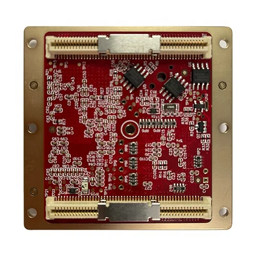
DIP Through Hole PCB Assembly
Name: DIP Through Hole Pcb Assembly
Substrate: FR-4/CEM-1/CEM-3/Polyimild/PTFE/Rogers
Copper Thickness: 1/3OZ- 6OZ
Plate thickness: 0.21-6.0mm
minute. Hole size: 0.20mm
minute. Line width: 4 million
minute. Line spacing: 0.075 mm
Surface treatment: spray tin/gold drill/OSP/lead-free spray tin
Board size: minimum 10*15mm, maximum 508*889mm
Product Type: OEM&ODM
PCB standard: IPC-A-610 D/IPC-III standard
Certificate: ISO9001/ CE//TUV/ ROHS
Warranty: 1 year
Service: One-stop turnkey service
Electronic testing: 100%
Logistics: Air/Sea
DIP package is the abbreviation of dual inline-pin package, also known as dual inline package technology, dual-inline package, a component package form of DRAM. Refers to integrated circuit chips packaged in dual-in-line form. Most small and medium-sized integrated circuits use this package, and the number of pins generally does not exceed 100.
Introduce
The DIP-packaged CPU chip has two rows of pins and needs to be inserted into a chip socket with a DIP structure. Of course, it can also be directly inserted into a circuit board with the same number of solder holes and geometric arrangement for soldering. When plugging and unplugging chips in DIP packages from the chip socket, special care should be taken to avoid damage to the pins. DIP package structures include: multi-layer ceramic dual in-line DIP, single-layer ceramic dual in-line DIP, lead frame DIP (including glass ceramic sealing type, plastic encapsulation structure type, ceramic low-melting glass encapsulation type) Wait.
Features
Suitable for perforation soldering on PCB (printed circuit board), easy to operate.
The ratio between the chip area and the package area is large, so the volume is also large.
The earliest 4004, 8008, 8086, 8088 and other CPUs all used DIP packages, through which the two rows of pins can be inserted into the slots on the motherboard or soldered on the motherboard.
In the era when memory particles were directly inserted on the motherboard, DIP packaging was once very popular. DIP also has a derivative method SDIP (Shrink DIP, shrinking double-entry package), which has a pin density six times higher than DIP.
DIP is also the abbreviation of DIP switch, and its electrical characteristics are:
1. Electrical life: each switch is tested under voltage 24VDC and current 25mA, and can be toggled back and forth 2000 times;
2. Rated current for infrequent switching: 100mA, withstand voltage 50VDC;
3. The rated current of the switch is often switched: 25mA, withstand voltage 24VDC;
4. Contact resistance: (a) The initial value is up to 50mΩ; (b) The maximum value after the test is 100mΩ; 5. Insulation resistance: Minimum 100mΩ, 500VDC;
6. Compressive strength: 500VAC/1 minute;
7. Interpolar capacitance: maximum 5pF;
8. Circuit: single contact single selection: DS(S), DP(L).
In addition, the digital aspect of the film
DIP (Digital Image Processor) two-dimensional actual image
Use
The chip with this packaging method has two rows of pins, which can be directly soldered on the chip socket with DIP structure or soldered in the soldering position with the same number of soldering holes. Its feature is that it can easily realize the perforation welding of the PCB board, and has good compatibility with the main board. However, due to its relatively large package area and thickness, and the pins are easily damaged during the plugging and unplugging process, the reliability is poor. At the same time, due to the influence of the process, this packaging method generally does not exceed 100 pins. With the high integration inside the CPU, the DIP package quickly withdrew from the stage of history. Their "footprint" can only be seen on old VGA/SVGA graphics cards or BIOS chips.
We support DIP Through Hole PCB Assembly business, Kingford is a professional one-stop PCBA service factory, welcome to place an order

Name: DIP Through Hole Pcb Assembly
Substrate: FR-4/CEM-1/CEM-3/Polyimild/PTFE/Rogers
Copper Thickness: 1/3OZ- 6OZ
Plate thickness: 0.21-6.0mm
minute. Hole size: 0.20mm
minute. Line width: 4 million
minute. Line spacing: 0.075 mm
Surface treatment: spray tin/gold drill/OSP/lead-free spray tin
Board size: minimum 10*15mm, maximum 508*889mm
Product Type: OEM&ODM
PCB standard: IPC-A-610 D/IPC-III standard
Certificate: ISO9001/ CE//TUV/ ROHS
Warranty: 1 year
Service: One-stop turnkey service
Electronic testing: 100%
Logistics: Air/Sea
