
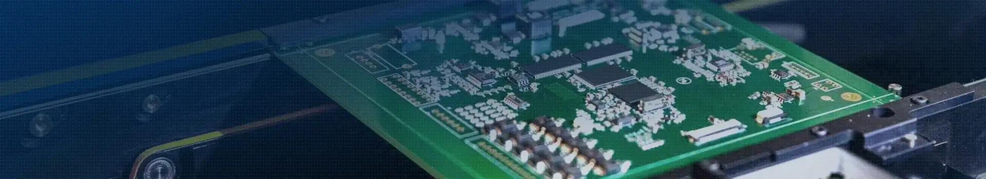
Professional PCB manufacturing and assembly
Building 6, Zone 3, Yuekang Road,Bao'an District, Shenzhen, China
+86-13410863085Mon.-Sat.08:00-20:00
| Item | Manufacturing Capability |
| PCB Layers | 1~64 Layer |
| Quality Grade | IPC Class 2|IPC Class 3 |
| Laminate/Base material | FR-4|S1141|High Tg|PTFE|Ceramic PCB|Polyimide|S1000-2|IT180A|Isola-FR408HR|FR406|Isola 370 HR|Rogers|Taconic|Arlon|Halogen Free, etc. |
| Brand of Laminate | Kingboard|ITEQ|Shengyi|Nanya|Isola|TUC|SYL|Arlon|Nelco|Taconic|Hitachi|Rogers, etc. |
| High Temperature Material | Normal Tg: Shengyi S1141|KB6160|Huazhen H140(not suitable for lead-free process ) |
| Middle Tg: For HDI、multilayers: SY S1000H|ITEQIT158|HuazhengH150|TU-662|SY S1150G|HuazhengH150HF|H160HF; | |
| High Tg: For thick copper、high layer: SY S1000-2|ITEQIT180A|HuazhengH170|ISOLA: FR408R|370HR|TU-752|SY S1165 | |
| High Frequency Circuit Board Material | Rogers|Arlon|Taconic|SY SCGA-500|S7136|HuazhengH5000 |
| High Speed PCB Material | SY S7439|TU-862HF|TU-872SLK|ISOLA: I-Speed, I-Tera@MT40|Huazheng:H175|H180|H380 |
| Ink | Taiyo INK (Japan)|KUANGSHUN(China)|RONGDA(China)|Coates Screen(UK)|S.M Materials(Taiwan, China) |
| Heat Conductivity for Alu. Boards | 1.0 |
| Chemical | Rohm&Haas (US)|Atotech (Germany)|Umicore (Germany) |
| PCB Type and Services | Prototype PCB|Rigid PCB|Flexible PCB(FPC)|Rigid-Flex PCB|HDI PCB|High Tg PCB|BGA PCB|Impedance Control PCB|IMS PCB(LED PCB Board, Aluminum PCB, Metal Core PCB)|Multilayer PCB|PCBA(PCB Assembly Service) |
| Max Board Size | 609 * 889 mm |
| Board Thickness | 0.1~8.0mm |
| Board Thickness Tolerance | ±0.1mm / ±10% |
| Min base copper thickness | Outer layer:1/3oz (12um) ~10oz|Inner layer:1/2oz~6oz |
| Max finished copperthickness | 6 OZ |
| Min Mechanical Drilling Hole Size | 6mil(0.15mm) |
| Min Laser Drilling Hole Size | 3mil(0.075mm) |
| Min CNC Drilling Hole Size | 0.15mm |
| Hole Wall Roughness(Max) | 1.5mil |
| Min trace width/spacing(Inner Layer) | 2/2mil(Outer layer:1/3oz,Inner layer:1/2oz) (H/H OZ base copper) |
| Min trace width/spacing(Outer Layer) | 2.5/2.5mil (H/H OZ base copper) |
| Min spacing between hole to inner layer conductor | 6mil |
| Min spacing between hole to outer layer conductor | 6mil |
| Min annular ring for via | 3mil |
| Min annular ring for component hole | 5mil |
| Min BGA diameter | 8mil |
| Min BGA pitch | 0.4mm |
| Min Finished hole size | 0.15mm(CNC)|0.1mm(Laser) |
| Half Hole Diameter | Minimum Half hole Diameter: 1mm, Half hole is a special technology, so half hole diameter should be greater than 1mm. |
| Hole Wall Copper Thickness (Thinnest) | ≥0.71mil |
| Hole Wall Copper Thickness (Average) | ≥0.8mil |
| Minimum Air Gap | 0.07mm(3mil) |
| Fine SMD Pitch | 0.07mm(3mil) |
| Max aspect ratios | 20:01 |
| Min soldermask bridge width | 3mil |
| Soldermask/circuit processing method | Film|LDI |
| Min thickness for insulating layer | 2mil |
| HDI & special type PCB | HDI(1-3 steps)|R-FPC(2-16 layers)|High frequency mix-pressing(2-14 layers)|Buried capacitance & resistance … |
| Max. PTH (Round Hole) | 8mm |
| Max. PTH (Round Slot Holes) | 6*10mm |
| PTH Deviation | ±3mil |
| PTH Deviation (Width) | ±4mil |
| PTH Deviation (Length) | ±5mil |
| NPTH Deviation | ±2mil |
| NPTH Deviation (Width) | ±3mil |
| NPTH Deviation (Length) | ±4mil |
| Hole Position Deviation | ±3mil |
| Character Types | Serial Number|Barcode|QR Code |
| Min Character Width (Legend) | ≥0.15mm, Characters width less than 0.15mm will be unidentifiable. |
| Min Character Height (Legend) | ≥0.8mm, Characters height less than 0.8mm will be unidentifiable. |
| Character Width to Height Ratio (Legend) | 1:5, 1:5 is the most suitable ratio for production. |
| Distance between Trace and Outline | ≥0.3mm(12mil), Ship as individual boards: Distance between Trace and Outline ≥0.3mm, Ship as Panelized boards with V-cut: Distance between Trace and V-cut line ≥0.4mm |
| Panelization without Spacing | 0mm, Ship as Panelized boards and the spacing between boards is 0mm. |
| Panelization with Spacing | 1.6mm, Make sure the spacing between boards should be ≥1.6mm, otherwise it will be hard to process routing. |
| Surface Finishes | OSP|HASL|HASL Lead-Free (HASL LF)|Immersion Silver|Immersion Tin|Plated Gold|Immersion Gold(ENIG)|ENEPIG|Golden Finger+HASL|ENIG+OSP|ENIG+Golden Finger|OSP+Golden Finger, etc. |
| Solder-Mask Finishing | (1). Wet Film (LPI Soldermask) |
| (2). Peelable Soldermask | |
| Solder Mask Colors | Green|Red|White|Black, Blue|Yellow|Orange|Purple, Gray|Transparent .etc. |
| Matte: Green|Blue|Black, etc. | |
| Silkscreen Colors | Black|White|Yellow, etc. |
| Electrical Testing | Fixture / Flying Probe |
| Other Testing | AOI, X-Ray(AU&NI), Two-dimension Measurement, Hole Copper Instrument, Controlled Impedance Test(Coupon test&Third Party Report), Metalloscope, Peeling Strength Tester, Solderability Test, Logic Contamination Test |
| Profile | (1). CNC Routing (±0.1mm) |
| (2). CNC V-Cut(±0.05mm) | |
| (3). Bevelling | |
| (4). Mould-Die Punching(±0.1mm) | |
| Special Capabilities | Thick Copper, Thick Gold(5U”), Gold Finger, Blind and Buried Hole, Countersink Hole, Semi-hole, Peelable Mask, Carbon Ink, Counter sink hole, Plated board edge, Press fit hole, Control depth hole, VIA in PAD, Non-conductive resin plug hole, Plating plug hole, Coil PCB, Super Mini PCB, Peelable Mask, Controlled Impedance PCB, etc. |

Just upload Gerber files, BOM files and design files, and the KINGFORD team will provide a complete quotation within 24h.