
Professional PCB manufacturing and assembly
Building 6, Zone 3, Yuekang Road,Bao'an District, Shenzhen, China
+86-13410863085Mon.-Sat.08:00-20:00

The milling technology of PCB NC milling machine includes tool direction selection, compensation method, positioning method, frame structure and cutting point. These two aspects are important aspects to ensure milling accuracy.
1. Cutting direction and compensation method
When the milling cutter cuts into the plate, one side to be cut always faces the cutting edge of the milling cutter, and the other side always faces the cutting edge of the milling cutter. The former has smooth surface and high machining accuracy. The spindle always rotates clockwise. Therefore, whether it is a CNC milling machine with fixed spindle motion or fixed spindle motion, when milling the outer contour of PCB, the tool must move counterclockwise. This is often referred to as up milling. When milling the frame or groove inside the PCB, climb milling is used. Milling compensation means that the machine tool automatically installs the set value in the milling process, so that the milling cutter automatically offsets from the center of the milling line to set half the diameter of the milling cutter, that is, the radius distance, so as to keep the milling shape set by the program consistent. At the same time, if the machine tool has the compensation function, pay attention to the compensation direction and program commands. If the compensation command is not used properly, the shape of the circuit board will be more or less equal to the length and width of the milling cutter diameter.
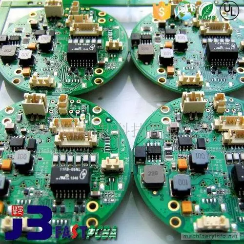
Circuit board
2. Positioning method and cutting point
The positioning methods can be divided into two types; One is internal positioning, the other is external positioning. Positioning is also very important for process planners. In general, the positioning plan should be determined during the pre production of PCB.
Internal positioning is a general method. The so-called internal positioning is to select the PCB mounting hole, jack or other non-metallic holes as the positioning holes. The relative position of the holes shall be on the diagonal line, and the holes with the largest diameter shall be selected. Metalized holes shall not be used. Because the difference in the thickness of the coating in the hole will affect the consistency of the positioning hole you select. At the same time, it is easy to damage the coating in the hole and the edge of the hole when taking the plate. On the premise of ensuring PCB positioning, the number of pin pcbs shall be as small as possible. Generally speaking, the small board uses 2 pins and the large board uses 3 pins. Its advantages are accurate positioning, small shape deformation, high precision, good shape and fast milling speed. Disadvantages: There are many types of holes in the plate, and pins with different diameters need to be prepared. If there are no locating holes available in the circuit board, it will be more troublesome to discuss with the customer about adding locating holes in the circuit board during preliminary production. At the same time, for each type of plate, different management of milling template is troublesome and expensive.
External positioning is another positioning method, which uses the positioning hole outside the plate as the positioning hole of the milling plate. Its advantage is easy to manage. If pre production specifications are good, there are usually about 15 milling templates. Because of the use of external positioning, the board cannot be milled and cut at one time, otherwise the PCB is easily damaged, especially the wire saw, because the milling cutter and dust collector will bring the board out, causing PCB damage and milling cutter fracture. Use the method of sectional milling to leave the joint, and first mill the plate. After the milling is completed, the program is suspended, and then the plate is fixed with tape. Carry out the second part of the procedure and drill out the connection point with a 3mm to 4mm drill bit. Its advantages are low template cost and easy management. It can mill all circuit boards without installing holes and locating holes. It is convenient for small craftsmen to manage. In particular, it can simplify the production of CAM and other early production personnel, while optimizing the pcb substrate. Utilization. The disadvantage is that due to the use of drill bits, the PCB shape has at least 2-3 convex points, which may


Just upload Gerber files, BOM files and design files, and the KINGFORD team will provide a complete quotation within 24h.