
Professional PCB manufacturing and assembly
Building 6, Zone 3, Yuekang Road,Bao'an District, Shenzhen, China
+86-13410863085Mon.-Sat.08:00-20:00


PCBA chip processing and assembly method and production process
With the development trend of electronic PCBA patch processing and assembly towards practicality and high assembly density, SMT surface patch technology has now become the mainstream technology for electronic component assembly. However, due to the excessive size of some electronic components in the PCBA patch processing and assembly process, software processing has not been replaced, and still plays a key role in the assembly process of electronic devices, so there will be certain components in the PCB circuit board. The total number of buried hole electronic devices. The assembly of both plug-in electronic devices and surface-mounted electronic devices is called mixed assembly, commonly known as mixed placement, and all assembly using surface-mounted electronic devices is called full-surface patch.
The key to the PCBA chip processing and assembly method and production process lies in the types of assembled electronic devices and the standards of assembled machinery and equipment. It can be roughly divided into four types: single and double-sided patch processing technology, single-sided and double-sided mixed placement processing technology, double-sided patch processing technology and double-sided mixed placement processing technology.
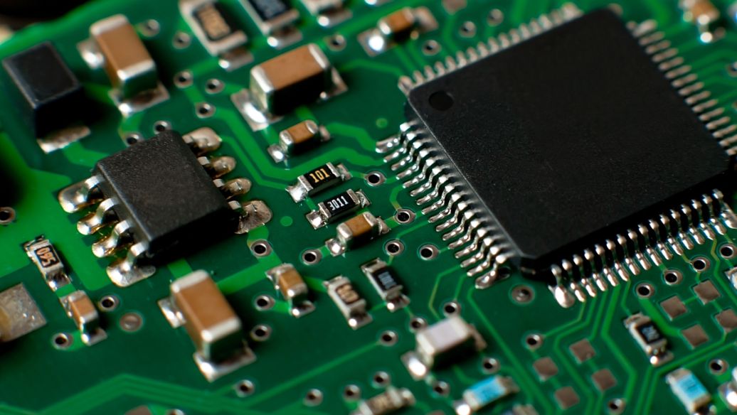
Single-sided and double-sided SMD means that all electronic components are SMD electronic components, and the electronic components will be assembled on one side of the PCB. Key steps of single and double-sided patch processing technology: finished product inspection and inspection → silk screen printing ink solder paste (or point patch glue) → patch → flow back welding → cleaning → inspection → maintenance.
PCBA patch processing is the process of assembling and welding PCB bare boards. As long as you grasp a few major processes, their process is not difficult to understand. Solder paste printing process, mounting process, and reflow soldering process are the three major processes in the chip processing process.
The PCBA patch processing process is as follows:
Chip processing link: solder paste printing—SPI solder paste inspection—SMT placement machine—online AOI—reflow soldering—offline AOI, transfer to DIP plug-in link: material forming—wave soldering—manual soldering—board washing, transfer to test assembly Links: quality inspection - programming - testing - assembly - QA inspection - packaging - delivery.
Some specific steps in the PCBA patch processing process:
1. According to the customer's Gerber file and BOM list, make the process file of SMT production, and generate the SMT coordinate file
2. Check whether all production materials are ready, make a complete set of orders, and confirm the PMC plan for production
3. Carry out SMT programming, and make the first board for verification to ensure that it is correct
4. According to the SMT process, make laser steel mesh
5. Carry out solder paste printing to ensure that the printed solder paste is uniform, thick and consistent
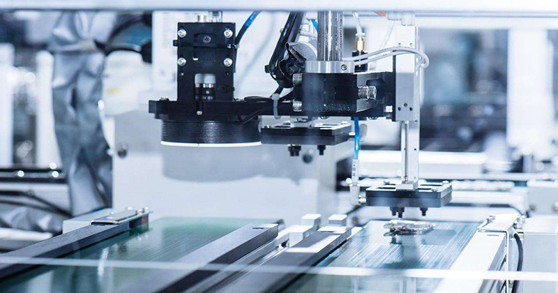
6. Use the SMT placement machine to mount the components on the circuit board, and perform online AOI automatic optical inspection if necessary
7. Set the perfect reflow soldering furnace temperature curve, let the circuit board flow through the reflow soldering, the solder paste will transform from paste, liquid to solid, and good soldering can be achieved after cooling
8. After the necessary IPQC inspection
9. The DIP plug-in process passes the plug-in material through the circuit board, and then flows through wave soldering for soldering
10. Necessary post-furnace processes, such as cutting feet, post-welding, board surface cleaning, etc.
11. QA conducts a comprehensive inspection to ensure the quality is OK.
About Impedance Control of PCB
May 29,2023


Just upload Gerber files, BOM files and design files, and the KINGFORD team will provide a complete quotation within 24h.