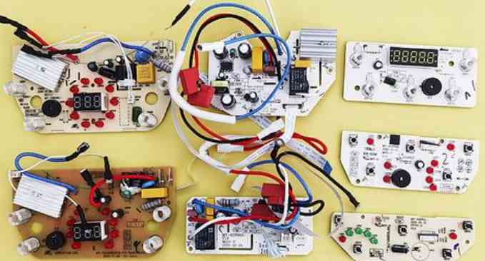
Detailed back drilling process in circuit board production
One, what is the circuit board back drill?
What is PCB circuit board back drilling? In fact, back drilling is a special kind of deep-control drilling. In the production process of PCB multilayer board, for example, the production of 12-layer circuit board, we need to connect the first layer to the ninth layer. Usually, we drill the through hole (one drill) and then sink copper. In this way, the 1st floor is directly connected to the 12th floor. Actually, we only need the 1st floor to connect to the 9th floor. The 10th to 12th floors are like a column because there is no line to connect them. This column affects the signal path and can cause signal integrity problems in communication signals. So drill this extra post (known in the trade as a STUB) off the reverse side (secondary drilling). So it's called back drilling, but it's usually not that clean, because the subsequent process electrolyzes a bit of copper, and the drill tip itself is sharp. Therefore, the circuit board manufacturer will leave a small point, the length of the STUB is called B value, generally in the range of 50-150UM.
What is a circuit board back drill
Two, what are the advantages of back drilling?
1. Reduce noise interference;
2. Local plate thickness becomes smaller;
3. Improve signal integrity;
4. Reduce the use of buried blind holes and reduce the difficulty of making PCB circuit boards.
Three, what is the role of the back drilling?
In fact, the role of back drilling is to drill out the PCB through hole segment that does not play any connection or transmission role, so as to avoid the reflection, scattering and delay of high-speed signal transmission, which brings "distortion" to the signal. The research shows that: In addition to the design, PCB board material, transmission line, connector and chip package, the main factors affecting the signal integrity of the signal system are the through hole has a great influence on the signal integrity.
Four, back drilling production principle
The micro-current generated when the drill needle contacts the copper foil on the substrate surface during drilling is used to induce the height position of the plate surface, and then drilling is carried out according to the set drilling depth. Drilling is stopped when the drilling depth is reached. The working diagram is shown in Figure 2
Working principle of back drilling production
Five, back drill production process?
1. Firstly, a circuit board is provided, and a positioning hole is provided on the circuit board. The positioning hole is used to position the PCB circuit board and drill a hole.
2. Electroplating the circuit board after drilling a drill, and dry film sealing treatment of the positioning hole before electroplating;
3. Make the outer graphic on the electroplated circuit board;
4. After the formation of the outer graphic on the PCB circuit board graphic plating, in the graphic plating before the positioning hole dry film sealing treatment;
5. Use the positioning hole used by the first drill to carry out back drilling positioning, and use the drill knife to carry out back drilling of the electroplating hole that needs to be backdrilled;
6. Wash the back borehole with water after back drilling to remove the drilling cuttings remaining in the back borehole.
Six, if there is a circuit board hole requirements from the 14th layer to the 12th layer to drill how to solve it?

1. If the PCB board has A signal line on the 11th floor, and there are through holes at both ends of the signal line connected to the component surface and solder surface, components will be inserted on the component surface, as shown in the figure below, that is to say, on the line, signal transmission is transmitted from component A to component B through the signal line on the 11th floor.
2. According to the signal transmission situation described in point 1, the function of through hole in this transmission line is equivalent to that of signal line. If we do not carry out back drilling, the signal transmission route is shown in Figure 5.
3. From the figure described in point 2, we can see that in the transmission process, the solder surface to the through-hole section of the 11th floor does not play any link or transmission role. The presence of this section of through-hole is easy to cause reflection, scattering and delay of signal transmission, so back drilling is actually to drill out the through-hole segment that does not play any link or transmission role, so as to avoid the reflection, scattering and delay of signal transmission, which will bring distortion to the signal.
Due to certain tolerance control requirements on drilling depth and plate thickness tolerance, we cannot meet 100% of the customer's absolute depth requirements. Then, is it better to control the depth of back drilling deeper or shallower? Our view on technology is better shallow than deep, Figure 6.
Seven, what are the technical characteristics of the back drilling plate?
1. Most backboards are hard;
2. The thickness and diameter are relatively large;
3.PCB board size is large;
4. Plate thickness: more than 2.5mm;
5. General minimum bore diameter > =0.3mm;
6. Back drilling depth tolerance: +/-0.05MM;
7. The number of layers of PCB multilayer board is generally 8 to 50 layers;
8. The back hole is usually 0.2MM larger than the hole to be drilled out;
9. The outer circuit is less, most of which is the square design of crimping hole;
10. If back drilling is required to drill to Layer M, the minimum thickness of medium from layer M to layer M-1 (the layer below layer M) shall be 0.17MM.
Eight, the back drilling plate is mainly used in what field?
Backplanes are mainly used in communication devices, large servers, medical electronics, military, and aerospace. Because military and aerospace are sensitive industries, domestic backboards are usually provided by military and aerospace system research institutes, R&D centers or PCB manufacturers with strong military and aerospace backgrounds. In China, the demand for backplanes mainly comes from the communications industry, which is now growing in the field of communications equipment manufacturing.
Implement back drill file output in Allegro
1. First select the backdrill Net and define the length. On the menu bar, click Edit-Properties to open the Editproperty dialog, as shown in the following image:
2. In the pop-up menu: Manufacturing - NC - BackdrillSetupandAnalysis, the diagram below:
3. Backdrill can start at the top or Bottom. The connection pins on the high speed signal and the VIA need to be backdrilled. The Settings are as follows:
4. The drilling files are as follows:
5. Send the back drilling file together with the back drilling depth table to the PCB factory. The back drilling depth table needs to be filled in manually.


