
Professional PCB manufacturing and assembly
Building 6, Zone 3, Yuekang Road,Bao'an District, Shenzhen, China
+86-13410863085Mon.-Sat.08:00-20:00


* First determine the position with other PCB board or system interface components on the PCB board, must pay attention to the coordination between interface components (such as the direction of components, etc.).
* Because the volume of handheld products are small, the components are arranged very compact, so for the larger volume of components, must give priority to determine the corresponding position, and consider the problem of coordination between each other.
* Carefully analyze the circuit structure, the circuit for block processing (such as high frequency amplifier circuit, mixing circuit and demodulation circuit, etc.), as far as possible strong signal and weak signal separated, the digital signal circuit and analog signal circuit separated, complete the same function of the circuit should be arranged in a certain range, so as to reduce the signal loop area; The filter network of each part of the circuit must be connected nearby, which can not only reduce the radiation, but also reduce the chance of interference, according to the anti-jamming ability of the circuit.

* Unit circuits are grouped according to their sensitivity to electromagnetic compatibility in use. Avoid interference sources (such as interference from the CPU on the data processing board) when arranging components that are vulnerable to interference in the circuit.
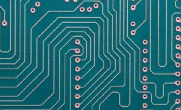
4 Wiring
After basically completing the layout of components, wiring can begin. The basic principle of wiring is as follows: after the assembly density permits, try to choose the low-density wiring design, and the signal routing thickness is as consistent as possible, which is conducive to impedance matching.
For radio frequency circuit, the unreasonable design of signal line strike, width and line spacing may cause cross interference between signal transmission lines. In addition, the system power supply itself also has noise interference, so in the design of RF circuit PCB must be considered comprehensively, reasonable wiring.
When routing cables, keep all the cables away from the PCB board frame (about 2mm) to avoid wire breakage or potential wire breakage. The power cord should be as wide as possible to reduce the loop resistance. At the same time, the direction of the power cord and ground wire should be consistent with the direction of data transmission to improve the anti-interference ability. The signal lines should be as short as possible and the number of holes should be minimized; The wires between components should be as short as possible to reduce the distribution parameters and electromagnetic interference between each other; For incompatible signal lines should be far away from each other, and try to avoid parallel lines, and the signal lines on both sides of the forward side should be mutually perpendicular; Wiring in the need of the corner of the address side should be appropriate to 135° Angle, avoid turning a right Angle.
Wiring and welding pad directly connected line should not be too wide, the line should be as far as possible away from the disconnected components, so as to avoid short circuit; The holes should be drawn on the components without buttocks, and should be far away from unconnected components as far as possible to avoid virtual welding, joint welding, and short circuit in production.
In the design of RF circuit PCB, the correct wiring of power cord and ground wire is particularly important, and reasonable design is the most important means to overcome electromagnetic interference. A considerable number of interference sources on PCB are generated through the power supply and ground wire, among which the ground wire causes the most noise interference.
The main reason that ground wire is easy to form electromagnetic interference is the impedance of ground wire. When there is a current flowing through the ground wire, it will generate voltage on the ground wire, resulting in the ground wire loop current, forming the ground wire loop interference. Common impedance coupling occurs when multiple circuits share a ground wire, resulting in what is called ground noise. Therefore, when wiring the ground wire of RF circuit PCB, it should be done:
* First, the circuit is divided into blocks. The RF circuit can be basically divided into high-frequency amplification, mixing, demodulation, local vibration and other parts. A common potential reference point, namely the ground wire of each module circuit, should be provided for each circuit module, so that signals can be transmitted between different circuit modules. Then, the summary in the RF circuit PCB access ground, that is, the summary in the general ground. Since there is only one reference point, there is no common impedance coupling and therefore no mutual interference problem.
* The digital area and the analog area should be isolated as far as possible, and the digital and analog ground should be separated, and finally connected to the power source.
* The ground wire inside each part of the circuit should also pay attention to the principle of single point grounding, minimize the area of the signal loop, and connect with the address of the corresponding filter circuit.
* If space permits, it is better to isolate each module with ground wire to prevent signal coupling effect between each other.
5 Conclusion
The key of RF circuit PCB design is how to reduce the radiation ability and how to improve the anti-interference ability, reasonable layout and wiring is the guarantee of the design of RF circuit PCB. The method mentioned in this paper is helpful to improve the reliability of RF circuit PCB design, solve the problem of electromagnetic interference, and achieve the purpose of electromagnetic compatibility.
What kind of circuit board does the sensor need
Apr 02,2023


Just upload Gerber files, BOM files and design files, and the KINGFORD team will provide a complete quotation within 24h.