
Professional PCB manufacturing and assembly
Building 6, Zone 3, Yuekang Road,Bao'an District, Shenzhen, China
+86-13410863085Mon.-Sat.08:00-20:00

Many friends who have PCB copying board demand are curious about how to calculate the cost of PCB copying board. Shenzhen kingford is a professional PCB copying board proofing manufacturer with many years of PCB copying board experience. Copying board products cover industrial control, security, smart home, medical and other industrial electronic products. Next, I will introduce how to calculate the cost of PCB copying board.
PCB copying board cost, the general quotation method in the industry is based on the need to copy the board on the circuit board of the PIN (PIN) number, the number of lines, screen printing and so on and combined with the PCB board difficulty to calculate. The cost of PCB copying board should refer to the size of PCB board, the number of PCB board layers, the density of components and the difficulty of operation.
How long does it take to copy PCB board?
PCB copying time is related to the number of PCB board layers, the number of welding inventory and the number of required data;
Simple board (100 welding spots within the double panel) the fastest can do within a day out of the data;
Complex boards (many devices, many layers, complex board structure) shall be delivered according to the physical evaluation of the sample.
What does PCB copy board need to provide?
Usually, simple single and double panel copying board only needs to provide a set of samples. If it is multi-layer board, it is best to provide two sets of exactly the same samples, which is convenient for later proofing and debugging samples.

Shenzhen kingford PCB copying capacity
Number of top floors: 38;
Maximum plate thickness: 6 mm ±0.05 mm(2 mil);
Maximum size: 640 mm × 480 mm ±0.1 mm(4 mil);
Minimum line width: 0.01mm (0.4mil) for hard plate / 0.005mm (0.2mil) ± 0.01mm (0.4mil) for flexible plate;
Minimum line clearance: hard plate 0.01mm (0.4mil)/ flexible plate 0.005mm (0.2mil) ± 0.01mm (0.4mil);
Minimum mechanical through-hole: 0.15 mm(6 mil) hard plate / 0.1 mm(4 mil) ±0.01 mm(0.4 mil) flexible plate;
Minimum mechanical holes: 0.15 mm(6 mil) for hard plate / 0.1 mm(4 mil) ±0.01 mm(0.4 mil) for flexible plate;
Minimum blind hole: hard plate 0.1mm (4 mil)/flexible plate 0.1mm (4 mil) ± 0.01mm (0.4mil);
Minimum laser hole: hard plate 0.1mm (4 mil)/flexible plate 0.1mm (4 mil) ± 0.01mm (0.4mil);
Blind hole types: 1st order, 2nd order, 3rd order, 4th order laser blind hole;
Type of buried hole: > 20 categories;
Multilayer copper thickness measurement: ± 1.7um (0.05oZ);
Multilayer thickness measurement: ±5 um(0.2 mil);
Impedance measurement: 5 ~ 150 Ω ±0.5Ω;
Resistance value measurement: 0.000001Ω ~ 20 MΩ ±5%;
Capacitance measurement: 0.001pF ~ 100F ±5%;
Inductance measurement: 0.001nH ~ 10H ±5%;
Magnetic bead equivalent resistance measurement: 10Ω ~ 2000 Ω(100MHz) ±10%;
Crystal frequency measurement: 1KHz ~ 200MHz ±1%;
Voltage regulator diode measurement: 0.5V ~ 56V ±0.01V.
PCB copy board service process
1. Customer provides product pictures or sample copy board;
2. Evaluate quotation according to pictures or samples and customer needs;
3. The customer confirms the quotation, signs the contract and pays the project deposit;
4. Received advance payment and arranged engineers to copy the board;
5. After copying the board, provide the screenshot of the document to the customer for confirmation;
6. The customer confirmed OK, settled the balance, and provided the information of copying the board.
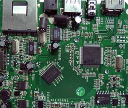
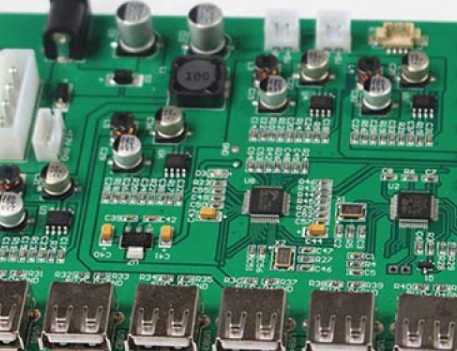
2. The best smt plant
Shenzhen kingford is one of the best smt SMT plants in Shenzhen. We can undertake small and medium-sized batch SMT SMT processing services, support processing of incoming materials and samples and OEM services. Our business covers PCB design, PCB board making, SMT/DIP welding and processing, assembly and testing one-stop PCBA services.
SMT patch processing capability
1. Maximum board card: 310mm*410mm(SMT);
2. Maximum plate thickness: 3mm;
3. Minimum plate thickness: 0.5mm;
4. Minimum Chip parts: 0201 package or parts above 0.6mm*0.3mm;
5. Maximum weight of mounted parts: 150g;
6. Maximum parts height: 25mm;
7. Maximum parts size: 150mm*150mm;
8. Minimum spacing of pin parts: 0.3mm;
9. Minimum ball parts (BGA) spacing: 0.3mm;
10. Minimum ball parts (BGA) ball diameter: 0.3mm;
11. Maximum parts mounting accuracy (100QFP) : 25um@IPC;
12. Patch capacity: 3-4 million points/day.
SMT patch processing process
1. Customers place orders
Customers place orders to smt plant according to their actual needs and put forward specific requirements. The processing plant will evaluate its capacity to see if it can fulfill the order. If the manufacturer is sure that they can complete the order within the expected time, then the two parties will negotiate to determine the production details.
2. Production materials provided by customers
After placing an order, the customer shall provide a series of documents and lists to the smt plant, such as PCB electronic files, coordinate files, BOM list and so on, which must be provided.
3. Purchase raw materials
smt plant will purchase related raw materials from designated suppliers according to the documents provided by customers.
4. Incoming material inspection
Before SMT processing, strict quality inspection shall be carried out for all raw materials to be used to ensure that they are qualified before being put into production.
5. SMT production
During SMT processing, in order to ensure the production quality, whether it is SMT or welding production, the manufacturer needs to strictly control the furnace temperature.
6. SMT test
smt plant conducts strict product testing and delivers PCB boards that pass the testing to customers.
7. Packaging after sale
After SMT processing is completed, the product will be packaged and handed over to the customer to complete the entire SMT processing.
Why kingford?
1. Strength guarantee
▪SMT workshop: We have imported SMT machines and several sets of optical inspection equipment, with a daily output of 4 million. Each process is equipped with QC personnel, who can keep an eye on product quality.
▪DIP production line: We have two wave-soldering machines, among which there are more than 10 old employees who have worked for more than three years. The skilled workers can weld all kinds of plug-in materials.
2. Quality assurance, cost-effective
▪ High-end equipment can stick precision shaped parts, BGA, QFN, 0201 materials. Can also template patch, loose material hand.
▪ Sample and size batch can be produced, proofing from 800 yuan, batch 0.008 yuan/point, no start-up fee.
3. Rich experience in SMT and welding of electronic products, stable delivery
▪ Accumulated SMT SMT processing services for thousands of electronic enterprises, involving many kinds of automotive equipment and industrial control motherboard. The products are often exported to Europe and the United States, and the quality can be affirmed by new and old customers.
▪ On time delivery, normal 3-5 days after complete materials, small batch can also be expedited on the same day shipment.
4. Strong maintenance ability and perfect after-sales service
▪ Experienced maintenance engineers can repair all kinds of patch welding caused by bad products, to ensure the connection rate of each piece of circuit board.
▪ 24-hour customer service staff at any time response, the fastest speed to solve your order problems.
PCBA proofing which good?
Mar 16,2023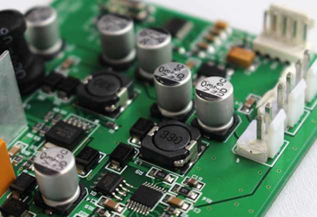


Just upload Gerber files, BOM files and design files, and the KINGFORD team will provide a complete quotation within 24h.