
Professional PCB manufacturing and assembly
Building 6, Zone 3, Yuekang Road,Bao'an District, Shenzhen, China
+86-13410863085Mon.-Sat.08:00-20:00

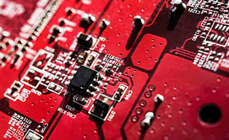
PCB board copying, that is, on the premise that there are physical electronic products and circuit boards, reverse analysis of circuit boards is carried out by using reverse R&D technology, and PCB files, bill of materials (BOM) files, schematic files and other technical documents of original products as well as PCB silkscreen production documents are carried out. 1: 1, and then use these technical documents and production documents for PCB board making, component welding, fly needle testing, circuit board debugging, and complete the complete copy of the original circuit board template.

What is a pulse power supply?
Common pulse current wave forms are square wave, triangle wave, saw tooth wave, step wave and so on. According to several principles of pulse waveform determination (such as accurate plating effect, easy analysis and research, easy to obtain and control, easy to popularize, etc.), the square wave is the most suitable pulse waveform. Typical square wave pulse waveform, as can be seen from Figure 1: pulse current is essentially a kind of on-off direct current.
Pulse power supply in the process of pulse electroplating, when the current conduction, pulse (peak) current is equivalent to ordinary DC current several times or even dozens of times, it is the instantaneous high current density of metal ions in extremely high over potential reduction, so that the sediment layer grain thinning; When the current is turned off, the discharge ions near the cathode region return to the initial concentration and the concentration polarization is eliminated, which is conducive to continue to use high pulse (peak) current density at the same time of the next pulse. At the same time, the phenomenon of recrystallization, absorption and desorption are also favorable to the sedimentary layer during the shutdown period. Such a process runs through the whole electroplating process synchronously and the mechanism contained therein constitutes the most basic principle of pulse electroplating. It has been proved that pulse power supply has more advantages than traditional DC electroplating in refining crystallization, improving physical and chemical properties of coating and saving precious metals
First, through slow energy storage, the primary energy has enough energy; The energy is then charged (or fed) to the intermediate storage and pulse forming system, which is then rapidly discharged to the load after some complex process of storage, compression, pulse formation, or conversion.
Note of pulse power supply:
Connection between pulse electroplating power source and plating bath conductor: The inductance of the connection between pulse electroplating power source and plating bath retards the current change, leading to delay the rise time of pulse current through the plating bath, resulting in pulse waveform distortion. The use of short, thick, more root cable, and negative and anode cable twisted together, can try to offset the inductance effect, reduce the distortion of pulse waveform, improve the quality of coating. Generally, the connection should not exceed 2m.
Selection of pulse electroplating power supply specifications and models: Generally, the peak current is indicated in the specifications and models of pulse electroplating power supply. For example, if the maximum current required is 10A and the maximum duty cycle used is 20%, the maximum peak current of pulse electroplating power supply is 10A/20%=50A.
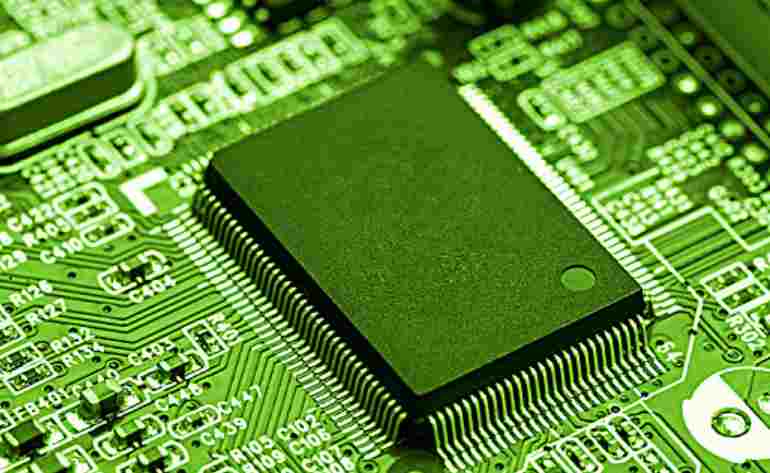
What tools are needed for PCB design
When thinking of tools, the images that usually come to mind are hammers, saws, welding tools, etc. But for printed circuit board design, the term "tool" is used differently. In most cases, PCB design tools include electronic software for Gerber and excellon files, CAD software, and the Internet for finding suitable sources. There are also materials that can be called "physical tools," such as formwork and welding tools.
Use PCB design tools
Engineers use all of the above tools and materials during the design and manufacturing phases of PCB construction. These phases begin when all the necessary materials have been allocated, the basic framework of the printed circuit board has been drawn and the appropriate grid has been drawn to understand how the PCB works.
l template
The stencil is a stainless foil used to apply the solder paste to the plate. The solder shield is used to prevent any excess solder paste from depositing on the selected area.
l soldering machine
Used to connect and secure all electronic components to the printed circuit board. Typically, welding machines include lead or tin solder.
L CAD software
Engineers use computer-aided design (CAD) software to move basic designs from paper to computers. The software is used to define schematics, components and connections within the PCB.
L Gerber file
Gerber is the file format used by engineers when creating drawings for the circuit board imaging process.
L Excellon file
This is also known as drill-down files. It is a file format used to control the size and position of finished holes on a printed circuit board. The Excellon file usually contains information regarding the drill string number, hole size and number, and whether or not the hole has been plated.
All of these tools are important when creating various layers and using different components to make printed circuit boards for complex applications.


Just upload Gerber files, BOM files and design files, and the KINGFORD team will provide a complete quotation within 24h.