
Professional PCB manufacturing and assembly
Building 6, Zone 3, Yuekang Road,Bao'an District, Shenzhen, China
+86-13410863085Mon.-Sat.08:00-20:00

Before introducing how to perform system functions for testing after PCBA processing, it's a good idea to look at how it has been done effectively in the past. The best way to learn about actual system testing for Chinese students is to visit PCBA processing plants where companies develop products with similar lifestyles and inspect the entire production line, from the circuit board to the shop floor to product packaging and shipping. The secret is that our teachers can experience the various activities of the product based on real life during the production and development process, which is very helpful in improving our understanding of how the board is produced. Next, we'll look at the workflow of PCBA handling functional requirements analysis and test data management.
1. Functional test plan
Prior to smt fabrication of circuit boards, we usually had dfm specifications in the design and development process. This will allow you to participate in the system-wide design education activities in the "Design for Testability" time management development program. It will clearly indicate which technical aspects of functional testing are primarily included in the schematic, pcb layout, and even the microcontroller code. Patch processing
For example, enterprise users can touch capacitive touch screens. What do you want the operating system to do? It can wake up the screen or turn on the led and tell the microcontroller to perform an action. This ability to operate requires that you have the correct voltage between all of these components, that capacitive touch sensors and leds are installed correctly, and that the microcontroller has been programmed and operated as intended. The functional test plan will guide the machining quality of the entire pcba board.
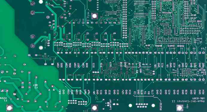
2. Test points
The test point is just a printed circuit board on a circuit board, so we designed it to be easy to test. Because of the main causes of various social problems in Chinese enterprises, you do not want to be able to develop relying on the pins or pads of the probe parts. The size of these pads is not specified, but should be large enough to make contact with the test probe.
3. System programming
If you look at the internal control structure of any complex product, you may find yourself with a programming connector or an empty spot on the PCB where you can place the programming connector. This connector is often considered by enterprise management to be directly used to study and learn programming for microcontroller design technicians mounted on printed circuit boards and therefore requires us to be referred to as "in-system". In the case of mass social production, the installation of magnetic heads is not educational. It can be used by designers mainly for debugging purposes, rather than installed in the production of economic development construction process to eliminate these business costs.
4. Test the fixture
For early Chinese prototypes or small designs, you can manually test each board as needed. You will thank yourself in the future for educating yourself to complete this exercise, as it allows you to appreciate and understand the capabilities and ways in which the business recognizes your products, market economy, normal operations, management, and accounting. Human societies are generally not good at repetition, so researching a system test plan, even with checkboxes, can help you avoid skipping any steps.

At this time, the processing parts of the electronic processing industry have been processed from the original to miniaturization. We now require smaller and smaller devices, thinner and lighter products, which will lead to smaller distance between parts and parts, and the pins and pads within the product will be closer and closer, and the gaps between the parts will become smaller and smaller, which will lead to pollutants blocked in the gaps. This means that small particles can cause a short circuit if they are attached between two pads or between parts. In recent years, the electronic assembly and processing industry for cleaning requirements are increasingly high, not only for the products we produce higher requirements, but also for environmental protection and everyone's health is also higher requirements, resulting in a lot of cleaning equipment suppliers, natural cleaning has become one of the main content of the electronic assembly and processing industry technical exchange. You may not know that PCBA proofing cleaning can improve the quality of the circuit board, if not cleaned, it may affect the stability of the product may also occur in the use of the product short circuit phenomenon, the following hundred thousand to explain to you the role of PCBA proofing cleaning.
1, three anti-paint coating requirements
You may not know that our PCBA proofing before the surface coating, if the resin residue on the surface of the patch is not removed, it will lead to the phenomenon of lamination or cracking of the product's protective layer; Without cleaning, the surfactant residue of the patch may cause electrons to migrate under the patch coating, resulting in the failure of the coating's crack protection. If we clean the patch before applying the tri-resistant paint, we can improve the adhesion rate of our coating.
2, no cleaning also need to be cleaned
By current inter-industry standards, what we mean by clean free is that the residues on the board are safe from a chemical point of view, will not have any effect on the board line, and can remain on the board. Corrosion, electromigration and other special testing methods can be used to determine the halogen/halide content in the product and then to determine the safety of the clean free components after assembly.
3. Appearance and electrical performance requirements
The most direct impact of PCBA proofing pollution is the appearance. If we use our proofing patches in a high temperature and humidity environment, we will find the problem. You can see that the residue on the product may absorb water and turn white. Due to the widespread use of lead-free chips, micro BGA, chip-level packaging and 01005 in the component process, these will reduce the distance between our components and the board, reduce the size, and increase the assembly density. If we find that halides are hidden under components that cannot be cleaned, only local cleaning may result in the release of halides which can be disastrous afterwards
How does PCBA process solder paste printing
Feb 04,2023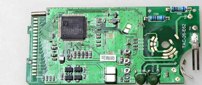


Just upload Gerber files, BOM files and design files, and the KINGFORD team will provide a complete quotation within 24h.