
Professional PCB manufacturing and assembly
Building 6, Zone 3, Yuekang Road,Bao'an District, Shenzhen, China
+86-13410863085Mon.-Sat.08:00-20:00

Four common surface treatment methods for high-frequency plate proofing
Circuit board manufacturing, circuit board design and PCBA processing manufacturers will explain four common surface treatment methods for high-frequency board proofing
High frequency circuit board is a special circuit board with high electromagnetic frequency. Generally speaking, high frequency can be defined as the frequency above 1GHz. Its physical performance, accuracy and technical parameters are very high, and are commonly used in automotive anti-collision systems, satellite systems, radio systems and other fields.
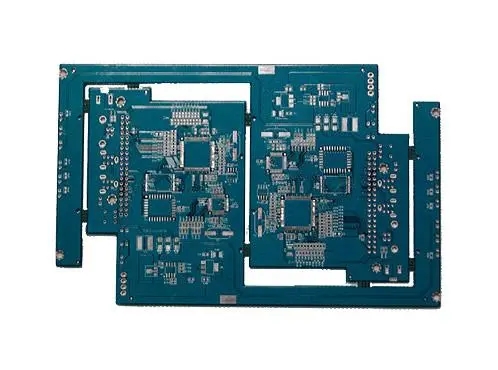
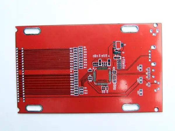
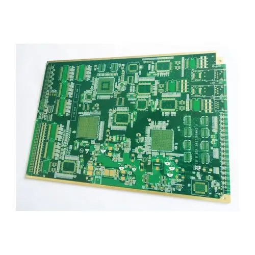
When making high-frequency boards, we will use a variety of surface treatment processes, such as some simple single panel/double-sided boards. Most of the surface treatment processes used are tin spraying or osp, and the high-frequency circuit boards with four or more layers use more gold deposition processes. Therefore, the surface treatment methods used in high-frequency board sampling are different. Each surface treatment method has its unique characteristics, taking silver as an example, Its manufacturing process is extremely simple. It is recommended to be used in lead-free welding and smt, especially for fine lines. The most important thing is to use chemical silver for surface treatment, which will greatly reduce the overall cost. Today we will introduce several common surface treatment methods for high-frequency plate proofing.
1. HASL hot air leveling (commonly known as tin spraying)
Tin spraying is a common treatment method in the early period of high-frequency circuit board proofing. Now it is divided into lead tin spraying and lead-free tin spraying. Advantages of tin spraying: After the high-frequency circuit board is completed, the copper surface is completely wetted (completely covered with tin before welding), which is suitable for lead-free welding. The process is mature and the cost is low, which is suitable for visual inspection and electrical testing. It is also one of the high-quality and reliable high-frequency circuit board proofing methods.
2. Chemical nickel gold
Nickel plated gold is a kind of surface treatment process for high-frequency circuit board proofing, which is widely used. Remember that nickel layer is a nickel phosphorus alloy layer, which can be divided into high phosphorus nickel and medium phosphorus nickel according to phosphorus content. Their applications are different, and their differences will not be introduced here. Advantages of nickel gold: suitable for lead-free welding; The surface is very flat, suitable for SMT, electrical testing, switch contact design, aluminum wire binding, thick plate, and strong resistance to environmental attacks.
3. Nickel palladium
Nickel palladium has gradually started to be used in the field of high-frequency circuit board proofing, and was previously used more in semiconductors. Suitable for binding with gold and aluminum wires. The advantage of using nickel palladium pcb board for proofing is that it is applied on IC carrier plate, suitable for gold wire binding, aluminum wire binding, and lead-free welding. Compared with ENIG, there is no nickel corrosion (black disc) problem, the cost is cheaper than ENIG and electronickel gold, and it is suitable for a variety of surface treatment processes and exists on the board.
4. Nickel gold electroplating
Electroplated nickel gold is divided into "hard gold" and "soft gold". Hard gold (such as gold cobalt alloy) is often used on gold finger (contact connection design), and soft gold is pure gold. Electroplated nickel gold is widely used on IC carrier plates (such as PBGA) and is mainly suitable for binding gold wire and copper wire. However, the IC carrier plate is suitable for electroplating, and the binding gold finger area needs additional conductor wires for electroplating. The advantage of electroplated nickel gold high-frequency circuit board proofing is that it is suitable for contact switch design and gold wire binding, and is suitable for electrical testing.
Circuit board manufacturing, circuit board design and PCBA processing manufacturers will explain four common surface treatment methods for high-frequency board proofing.


Just upload Gerber files, BOM files and design files, and the KINGFORD team will provide a complete quotation within 24h.