
Professional PCB manufacturing and assembly
Building 6, Zone 3, Yuekang Road,Bao'an District, Shenzhen, China
+86-13410863085Mon.-Sat.08:00-20:00


PCB and FPC flexible circuit board production solution
When the PCB surface is converted to lead-free type, the PCB needs to withstand extremely high welding temperature, and the thermal shock resistance of the surface solder mask is increasingly required The surface treatment of the terminal and the solver mask (ink, covering The peer length of the film) and the bonding force with the base partner are required to be higher and higher We need a better preprocessing of PCB to ensure its process By improving our technology to increase product output, we can gain profit growth points High quality pre-treatment agents can undoubtedly help us reduce costs
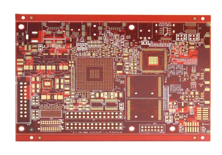
Preprocessing PCB
This paper mainly introduces the problems often encountered in the production process and the countermeasures. Rigid PCB and flexible PCB:
1. After dry film or wet film treatment of the line section, side corrosion and back corrosion will occur when etching the pipeline, resulting in insufficient line width or uneven lines The reason is the improper selection of dry and wet film data, improper exposure parameters, and poor performance of the exposure machine Nozzle adjustment of developing and etching parts, unreasonable adjustment of relevant parameters, improper concentration range of chemical solution, incorrect transmission speed, etc May cause problems However, we often find that there is no abnormality after checking the above parameters and the performance of related equipment However, problems such as over correction and
pitting of the circuit board still occur when the board is made. What is the root cause?

2. During the execution of PCB pattern electroplating, PCB, FPC terminal surface treatment, such as gold dipping, electrogilding, electrotinning, tin and other process treatment, we often find that the made PCB has leakage at the edges of dry film and wet film or solder mask Electroplating, or most of the board members, or some places, will bring unnecessary scrap or adverse consequences, which will bring unnecessary trouble to the post-processing, even the final waste, which is heartbreaking! Investigate the reason, everyone usually thinks of the dry film and wet film parameters, and the data efficiency is questionable; The solder mask, such as ink used for hardboard, has problems with the covering film used for soft board, or has problems with printing, pressing, curing and other stages Indeed, every place can cause this problem After checking the above steps, we are also confused. No problems or problems have been solved, but the seepage phenomenon still exists Is there any reason not found?
3. The circuit board will be tin tested before shipment. Of course, the customer will solder the components during use These two stages may occur, or at some stage, tin immersion or solder blistering may occur, and then the substrate is peeled off. Even when the tape is used to test the peel strength of the ink, when the peel strength of the flexible board covering film is tested by tension, the ink may appear The customer must not accept the obvious peeling or the insufficient or uneven peeling strength of the covering film, especially those who do precision surface mounting In the welding process, once the welding resistance film is shiny and peeled off, it will lead to inaccurate installation of the original parts, which will cause customers to lose a lot of components and work The circuit board factory will also face huge losses such as deduction, replenishment and even loss of customers Then, when we encounter such problems, what aspects do we usually work in? We usually analyze whether there is a problem with solder mask (ink, cover film) materials; Which there is a problem with the screen printing, lamination, and curing stage; Is there a problem with the plating solution? And more In this regard, we usually ask engineers to find out the causes from these chapters and make improvements We will also consider the weather? The weather has been relatively wet recently Does the board absorb water? (Both the base material and the barrier are easy to avoid noise) After some hard work, this problem is temporarily solved on the surface But this problem happened again unintentionally. Why? Check and improve the working parts that may have problems What have you not noticed?
Aiming at the puzzles and problems commonly existing in the PCB and FPC industries. We have carried out a lot of experiments and research, and finally found that the important reason for poor wiring, penetration, delamination, blistering and insufficient peel strength is the pretreatment part. It includes dry and wet film pretreatment, welding resistance treatment, electroplating pretreatment and other multi-stage pretreatment parts. Speaking of this, maybe many people in the industry can't help laughing. Pretreatment is the simplest, pickling, degreasing and micro etching. Many scientific and technical personnel in the industry know which pre-treatment agents, efficacy, parameters, and even formulas.


Just upload Gerber files, BOM files and design files, and the KINGFORD team will provide a complete quotation within 24h.