
Professional PCB manufacturing and assembly
Building 6, Zone 3, Yuekang Road,Bao'an District, Shenzhen, China
+86-13410863085Mon.-Sat.08:00-20:00

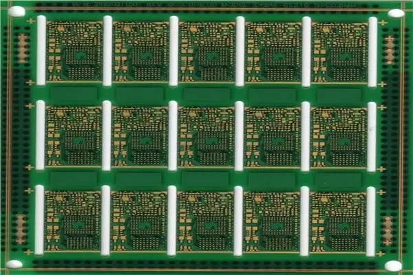
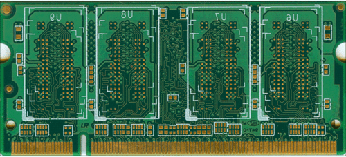
How to deal with PCB surface and how to produce high-quality PCB
In the order receiving process of our factory, customers often ask about different surface treatment of PCB and price. Therefore, today Xiaobian reorganizes the current mainstream surface treatment methods of PCB again for your reference.
1. Hot air leveling
The process of coating molten tin lead solder on the surface of PCB and leveling (blowing) it with heated compressed air makes it form a coating that is both resistant to copper oxidation and can provide good solderability. The copper tin metal compound is formed at the joint of solder and copper during hot air leveling, and its thickness is about 1-2 mil;
2. Organic oxidation protection (OSP)
On the clean bare copper surface, an organic film is grown chemically. This film has oxidation resistance, heat shock resistance and moisture resistance to protect the copper surface from further rusting (oxidation or vulcanization, etc.) in normal environment; At the same time, it must be easily removed by the flux in the subsequent welding high temperature for welding;
3. Electroless nickel gold precipitation
Wrap a thick layer of nickel gold alloy with good electrical properties on the copper surface and protect PCB for a long time. Unlike OSP, which is only used as a rust proof barrier, it can be useful in the long-term use of PCB and achieve good electrical performance. In addition, it also has the environmental tolerance that other surface treatment processes do not have;
4. Chemical silver precipitation
Between OSP and electroless nickel plating/gold leaching, the process is simple and fast. Exposed to heat, humidity and pollution, it can still provide good electrical performance and maintain good solderability, but it will lose luster. Because there is no nickel under the silver layer, silver deposition does not have all the good physical strength of electroless nickel plating/gold immersion;
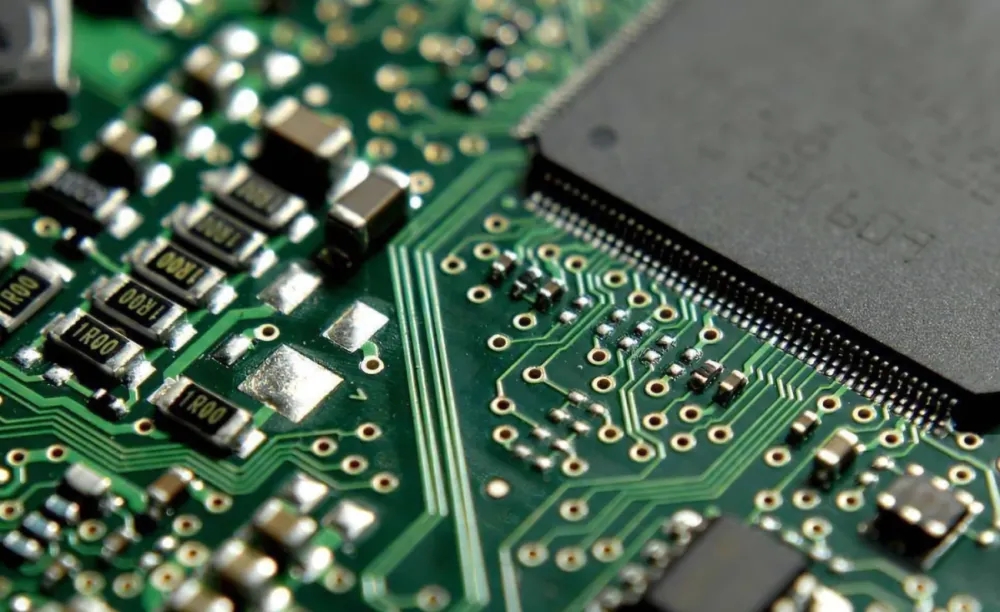
5. Nickel gold electroplating
The conductor on the PCB surface is plated with a layer of nickel first, and then a layer of gold. Nickel plating is mainly used to prevent the diffusion between gold and copper. Now there are two types of nickel gold plating: soft gold plating (pure gold, gold indicates that it looks dull) and hard gold plating (the surface is smooth and hard, wear-resistant, containing cobalt and other elements, and the surface looks bright). Soft gold is mainly used to make gold wire during chip packaging; Hard gold is mainly used for electrical interconnection at non welding points (such as gold finger).
6. Mixed Surface Treatment Technology for PCB
Two or more surface treatment methods are selected for surface treatment. The common forms are: nickel gold deposition+oxidation prevention, nickel gold electroplating+nickel gold deposition, nickel gold electroplating+hot air leveling, and nickel gold deposition+hot air leveling.
In all surface treatment forms, hot air leveling (lead-free/leaded) is the most common and cheapest, but please pay attention to the RoHS regulations of the European Union.
RoHS: RoHS is a mandatory standard formulated by EU legislation. Its full name is the Restriction of Hazardous Substances. This standard has been officially implemented since July 1, 2006. It is mainly used to regulate the material and process standards of electronic and electrical products, making them more conducive to human health and environmental protection. The standard aims to eliminate six substances including lead, mercury, cadmium, hexavalent chromium, polybrominated biphenyls and polybrominated diphenyl ethers in electrical and electronic products, and focuses on the provision that the content of lead shall not exceed 0.1%.
PCB manufacturers, PCB designers and PCBA processors will explain how PCB surfaces are treated and how to produce high-quality PCBs.


Just upload Gerber files, BOM files and design files, and the KINGFORD team will provide a complete quotation within 24h.