
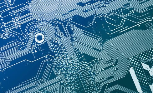
Professional PCB manufacturing and assembly
Building 6, Zone 3, Yuekang Road,Bao'an District, Shenzhen, China
+86-13410863085Mon.-Sat.08:00-20:00

Pcb and cutting size
① Maximum panel size: 530 * 622mm (tin plate: 450 * 622mm/MAX, depending on equipment capacity)
② Pay attention to the longitude and latitude of boardswith more than six layers (must be the same), which is easy to cause poor compression.
③ Size of reserved surface of multilayer PCB board (8-10 layers of 4-layer board 10-15 more than 6 layers of mm)
④ Commonly used copper core plate (0.2-3.2mm under 0.1mm radian), but not copper core plate (0.05-1.75mm radian)
Inside/outside
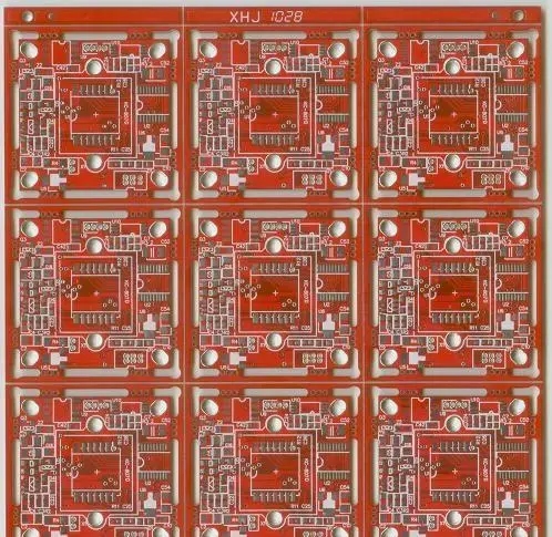
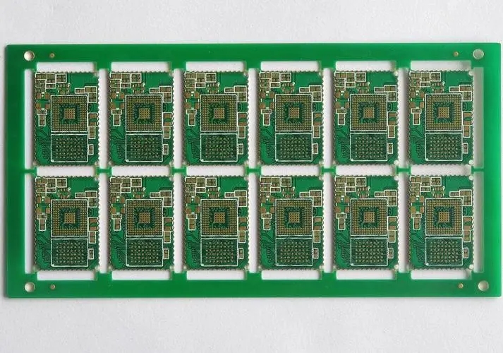
Pcb circuit board proofing
① 0.03mm (Hoz) compensation, copper thickness increases by 1oz, compensation increases by 0.025mm
② Width requirement of welding ring Hoz 0.15mm pth 0.18 (limit 0.13 0.16)
1 oz (0.17 mm depth 0.20) (limit 0.15 0.18)
2 oz (0.19 mm depth 0.22) (0.17 0.20 limit)
Copper thickness increases by 1 oz, compensation increases by 0.02 mm
③ Cutting copper wire: ensure the minimum wire distance: 0.4mm 0.15mm from copper wire (0.3mm from PAD and wire)
Copper hole: 0.250mm wire: 0.15mm pad: 0.2mm four layer plate
Copper hole: 0.250mm Wire: 0.18mm Pad: 0.2mm above the six layer plate
The copper wires produced in the copper extraction process must be removed, and the holes in the copper sheet must also be filled.
For loopless pth and NPth holes, 0.2mm copper shall be cut on one side. If the spacing cannot be ensured, drill twice.
PCB proofing
Proofing is the early stage of mass production. Only when the calibration is accurate, can batch production be put into batch production. Then, it is very important to provide accurate proofreading documents. Does everyone know what documents need to be provided? What problems should we pay attention to in the documents provided? Today, the editor will share with you:
First, you need to provide a PCB or GERBER file for HDI board proofing. The document shall include plate making instructions, including specific requirements for layers, materials, rubber pad technology, ink color, etc. Let's have a detailed understanding of some main parameters.
Materials: To illustrate the materials required for PCB production, FR4 is most commonly used at present, and the main material is epoxy resin peeling fiber cloth board.
Number of layers: It is necessary to specify the number of layers of PCB board. (The price of PCB varies with the number of layers, and the proofing process of PCB is the same.)
Color of solder mask: There are many colors, which can also be selected according to requirements, generally green.
Silk screen color: The color of silk screen font and border printed on HDI board proofing PCB is usually white.
Copper thickness: Generally, the copper thickness is calculated scientifically according to the current of PCB circuit. Generally, the thicker the better, but the cost will be higher, so a reasonable balance is required.
Whether the through-hole is covered by solder resist: PCB solder resist layer should insulate the through-hole, otherwise the through-hole is not insulated.
Surface coating: tin spraying and gold plating.
Quantity: The number of PCBs produced shall be clearly stated.


Just upload Gerber files, BOM files and design files, and the KINGFORD team will provide a complete quotation within 24h.