
Professional PCB manufacturing and assembly
Building 6, Zone 3, Yuekang Road,Bao'an District, Shenzhen, China
+86-13410863085Mon.-Sat.08:00-20:00


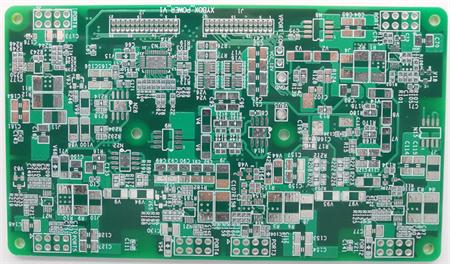
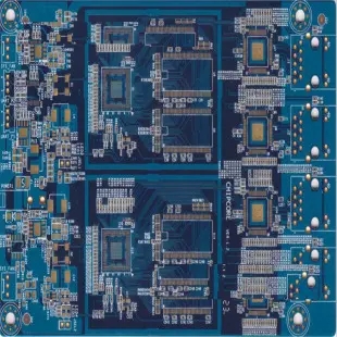
PCB circuit open and short circuit is a problem that PCB manufacturers encounter almost every day. It has been puzzling production and quality management personnel, causing insufficient shipments and replenishment, affecting on-time delivery, and leading to customer complaints. It is a difficult problem for insiders to solve.

The cause analysis and improvement methods of the above phenomena are listed as follows:
1、 Open circuit caused by exposed substrate
1. The copper clad laminate is scratched before entering the warehouse;
2. The CCL is scratched in the process of cutting;
3. The copper clad plate was scratched by the drill bit during drilling;
4. The copper clad plate is scratched in the process of transportation;
5. The copper foil on the surface was damaged due to improper operation when stacking plates after copper deposition;
6. The copper foil on the surface of the production plate is scratched when passing the leveler;
Improvement method:
1. The IQC must carry out spot check on the CCL before entering the warehouse to check whether there is scratch on the board surface and the base material is exposed. If there is, contact the supplier in time and make appropriate treatment according to the actual situation.
2. The copper clad plate was scratched during the blanking process, mainly because there were hard and sharp objects on the table of the blanking machine. During blanking, the copper foil was scratched and exposed due to the friction between the copper clad plate and the sharp objects. Therefore, the table must be carefully cleaned before blanking to ensure that the table is smooth and free of hard and sharp objects.
3. After copper sinking and full plate electroplating, the plates were scratched due to improper operation when stacking them: after copper sinking and full plate electroplating, when storing the plates, the plates were stacked together and then laid down, and when there were a certain number of plates, the weight was not light, the plate angle was downward and there was a gravitational acceleration, forming a strong impact force hitting the plate surface, causing the plate surface to scratch and expose the substrate.
4. The production plate is scratched when passing the leveler: the baffle of the plate grinder sometimes contacts the plate surface, and the edge of the baffle is uneven with sharp objects protruding, so the plate surface is scratched when passing the plate; The stainless steel transmission shaft becomes a sharp object due to damage, and the copper surface is scratched when passing the plate, exposing the base material.
5. The copper clad laminate was scratched by the drill bit when drilling, mainly because the spindle clamp bit was worn, or there were sundries in the clamp bit that were not cleaned, the drill bit could not be grasped firmly, the drill bit did not reach the top, which was slightly longer than the set drill bit length, the lifting height during drilling was not enough, and the drill bit tip scratched the copper foil when the machine tool moved, forming the phenomenon of exposed base material. The clamping nozzle can be replaced by the number of times recorded by grabbing the tool or according to the wear degree of the clamping nozzle; Clean the clamping nozzle regularly according to the operation procedures to ensure that there are no sundries in the clamping nozzle.
To sum up, it is easy to judge the scratch and exposure of the base material after copper deposition if the line is in the form of open circuit or line gap; If the scratch on the exposed substrate occurs before copper deposition, and when it is on the line, a layer of copper is deposited after copper deposition, the copper foil thickness of the line is significantly reduced, and it is difficult to detect in the subsequent open circuit and short circuit tests. In this way, the customer may burn the line due to the inability to withstand excessive current when using, and the potential quality problems and economic losses caused are considerable.
2、 Open circuit without hole
1. Sink copper is non porous;
2. There is oil in the hole to cause non porosity;
3. Excessive micro etching leads to non porosity;
4. Non porous due to poor electroplating;
5. The drilling nozzle burns the hole or the dust blocks the hole, resulting in non porosity;
Improvement measures:
1. Non porous copper sinking:
a. Pore free formation caused by the pore forming agent: It is due to the imbalance or failure of the chemical concentration of the pore forming agent. The role of the pore forming agent is to adjust the electrical properties of the insulating substrate on the hole wall, so as to facilitate the subsequent adsorption of palladium ions and ensure the complete coverage of chemical copper. If the chemical concentration of the pore forming agent is unbalanced or fails, it will lead to pore free formation.
b. Activator: the main ingredients are pd, organic acid, stannous ion and chloride. In order to deposit metal palladium evenly on the hole wall, it is necessary to control all the parameters to meet the requirements. Take our current activator as an example: the temperature is controlled at 35-44 ℃, which leads to insufficient density of palladium deposition and incomplete coverage of chemical copper; The material cost increases due to too fast reaction when the temperature is high. The concentration and colorimetry shall be controlled at 80% - 100%. If the concentration is low, the density of palladium deposition will be insufficient, and the chemical copper coverage will be incomplete; If the concentration is too high, the material cost will increase due to too fast reaction.
c. Accelerator: the main component is organic acid, which is used to remove stannous and chloride ion compounds adsorbed on the pore wall, revealing the catalytic metal palladium of the subsequent reaction. The chemical concentration of the accelerator we are using is controlled at 0.35-0.50N. If the concentration is high, the metal palladium is removed, resulting in incomplete chemical copper coverage. If the concentration is low, the effect of removing stannous and chloride ion compounds adsorbed on the pore wall is poor, resulting in incomplete coverage of subsequent chemical copper.
2. There is wet film oil left in the hole to cause non porosity:
a. When screen printing wet film, print a plate and scrape the screen bottom once to ensure that there is no oil accumulation on the screen bottom. Normally, there will be no residual wet film oil in the hole.
b. The 68-77T screen plate is used for silk screen wet film printing. If the wrong screen plate is used, such as ≤ 51T, wet film oil may leak into the hole. The oil in the hole may not be clean during development, and the metal layer will not be plated during electroplating, resulting in non porosity. If the mesh is high, the anti coating film may be broken by current during electroplating due to insufficient ink thickness, resulting in many metal points between circuits and even short circuits.
3、 Fixed position open circuit
1. Open circuit caused by scratch on the alignment film line;
2. Open circuit caused by trachoma on the alignment film line;
Improvement method:
1. The scratch on the alignment film line causes an open circuit. The film surface line is scratched by the friction between the film film surface and the board surface or garbage, causing light transmission. After development, the line at the scratch on the film is still covered by ink, causing anti plating during electroplating, and the line is corroded and open circuit during etching.
2. There are trachomas on the film film surface during alignment, and the lines at the film trachomas after development are still covered by ink, which causes anti plating during electroplating and open circuit due to erosion of the lines during etching. Belonging to Qinji Group, Baineng is a leading electronic industry service platform in China. It provides online components, sensor procurement, PCB customization, BOM distribution, material selection and other complete solutions for the electronic industry supply chain, meeting the comprehensive needs of small and medium-sized customers in the electronic industry in a one-stop manner.
4、 Anti plating open circuit
1. When developing, the broken dry film adheres to the circuit, causing an open circuit;
2. The circuit surface is attached with ink, causing open circuit;
Improvement methods
1. Open circuit caused by the adhesion of dry film fragments to the circuit:
A. The "drilling tail hole" and "silk screen hole" at the edge of the film or on the film are not completely sealed with light blocking adhesive tape. When exposed, the dry film at the edge of the plate is cured by light, and becomes a dry film fragment when developing, which falls into the developing solution or water washing tank. During subsequent plate passing, the dry film fragment attaches to the circuit on the plate surface, is resistant to plating, and forms an open circuit after film stripping and etching.
b. The nonmetallic hole masked with dry film breaks the dry film in the hole into pieces due to excessive pressure or insufficient adhesion during development and falls into the developing solution or water washing cylinder. The dry film fragments attach to the circuit during subsequent plate passing, resist plating during electroplating, and form an open circuit after film stripping etching.
2. There is ink attached to the circuit surface, which causes open circuit. The main reason is that when the ink is not pre baked or the amount of developing solution ink is too large, the ink attaches to the board surface, and then sticks to the rear transmission shaft or sponge water absorption roller. Later, when passing the PCB board, the ink attaches to the PCB, which is resistant to plating during electroplating, and forms open circuit after film stripping and etching.


Just upload Gerber files, BOM files and design files, and the KINGFORD team will provide a complete quotation within 24h.