
Professional PCB manufacturing and assembly
Building 6, Zone 3, Yuekang Road,Bao'an District, Shenzhen, China
+86-13410863085Mon.-Sat.08:00-20:00

1. First, there must be a reasonable direction:
Such as input/output, AC/DC, strong/weak signal, high frequency/low frequency, high voltage/low voltage, etc. Their direction shall be linear (or separate) and shall not be mixed with each other. Its purpose is to prevent mutual interference. The best trend is a straight line, but it is usually not easy to achieve. The worst trend is a circle. Fortunately, isolation can be improved. For DC, small signal, low voltage PCB design requirements can be lower. So "reasonable" is relative.
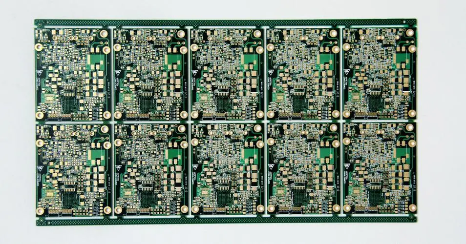
PCB factory processing circuit board
Circuit board
2. Select a good grounding point: the grounding point is usually the most important.
I don't know how many engineers and technicians have talked about a small grounding point, which shows its importance. Generally speaking, a common grounding is required. For example, multiple grounding wires of the forward amplifier should be combined and then connected to the main grounding. In fact, due to various restrictions, it is difficult to fully achieve this, but we should try our best to follow it. This problem is quite flexible in practice. Everyone has their own solution. It is easy to understand if it can be explained for a specific PCB.
3. Reasonably arrange power filter/decoupling capacitor.
In general, the schematic diagram only shows some power filters/decoupling capacitors, but does not indicate where they should be connected. In fact, these capacitors are used for switching devices (grid circuits) or other PCB components that require filtering/decoupling. These capacitors should be placed as close to these components as possible, and too far away will not affect them. Interestingly, when the power filter/decoupling capacitor is correctly arranged, the problem of grounding point is less obvious.
4. The line is exquisite, the line diameter is required, and the size of the buried hole is appropriate.
If conditions permit, the wide line shall not be thin; High voltage wire and high frequency wire shall be smooth without acute angle, and corners shall not be at right angles. The grounding wire should be as wide as possible, and it is better to use a large area of copper, which can greatly improve the problem of grounding points. The size of the pad or through hole is too small, or the size of the PCB pad does not match the size of the hole. The former is not conducive to manual drilling, while the latter is not conducive to CNC drilling. It is easy to drill the gasket into a "c" shape, but the gasket must be drilled out. The wires are too thin, and copper is not provided for large areas of non wiring areas, which can easily lead to uneven corrosion. That is to say, when the unknown area is corroded, the thin line is likely to be excessively corroded, or appears to have broken or completely broken. Therefore, the function of setting copper wire is not only to increase the area of ground wire and anti-interference ability.
5. Number of through-hole, solder joint and linear density.
Although there will be some problems in later production, these problems are caused by PCB design. They are: too many through-hole, and a little negligence in the copper sinking process will lay hidden dangers. Therefore, the design shall minimize wire holes. The density of parallel lines in the same direction is too large, so they can be easily connected together during welding. Therefore, the linear density shall be determined according to the welding PCB process level. The distance between welding points is too small, which is not conducive to manual welding. The welding quality can only be solved by reducing the working efficiency. Otherwise, hidden dangers still exist. Therefore, the minimum distance of welding spot shall be determined by comprehensively considering the quality and work efficiency of welding personnel.

On PCB drawing from welding Angle
Oct 24,2022


Just upload Gerber files, BOM files and design files, and the KINGFORD team will provide a complete quotation within 24h.