
Professional PCB manufacturing and assembly
Building 6, Zone 3, Yuekang Road,Bao'an District, Shenzhen, China
+86-13410863085Mon.-Sat.08:00-20:00


In the process of PCB design, many different methods can be taken to solve various problems. There are some adjustments of the design scheme itself, such as adjusting the layout of the line to reduce noise; There are also ways of laying out printed circuit boards. Design components can be installed automatically using layout tools, but manual adjustment of the automatic layout can help improve the quality of the board design. Through this measure, design rules testing will be aided by technical documentation to ensure that the design of the circuit board can meet the requirements of the circuit board manufacturer.
Separating the different layers of the board reduces associated capacitance, but this increases the number of layers of the board, which increases costs and creates more through-hole problems. Although the orthogonal grid power supply system and grounding circuit design may increase the physical size of the circuit board, it can effectively play the role of the grounding layer in the two-layer circuit board, reduce the capacitance and the complexity of the circuit board manufacturing.
Many PCB design tools can help engineers solve many problems at the beginning of the design process, but engineers still need to have a good understanding of the design requirements of printed circuit boards (PCBS). For example, if the editor of a printed circuit board (PCB) needs to know the number of layers of the board at the beginning of the design, for example, a two-layer circuit board needs to have a grounding layer and a power layer, which are composed of two independent layers. Automatic component layout technology is useful because it can help designers spend more time designing the layout area of the equipment. For example, power supply equipment can cause problems if it is too close to sensitive signal lines or areas with high temperatures. Similarly, signal wiring can be automated and avoid most of the problems, but analysis and manual manipulation of high-risk areas will help greatly improve the quality of printed circuit board (PCB) design, increase revenue, and reduce overall costs.
Design rule detection is also a very powerful tool for detecting lines to ensure that they are not too close together and that the loops are too short. However, the overall design still has a high economic value. The design planning inspection tool can also be used to detect and adjust the power layer and ground layer to avoid large areas of associated capacitance.
The above tools will also be of great assistance to Gerber and Excellon in their wiring and circuit board printing, as well as through hole drilling, in order to produce the final design product. In this way, the technical documentation is closely linked to the board manufacturer.

Conclusion:
Many problems need to be considered in PCB design process, PCB design tools can effectively deal with most of them. By adopting certain best practice guidelines, engineers can effectively reduce costs and improve board reliability, while meeting system specifications and bending system certification at a lower cost, thus avoiding further problems
The difference between PCB gold plate and gold plate
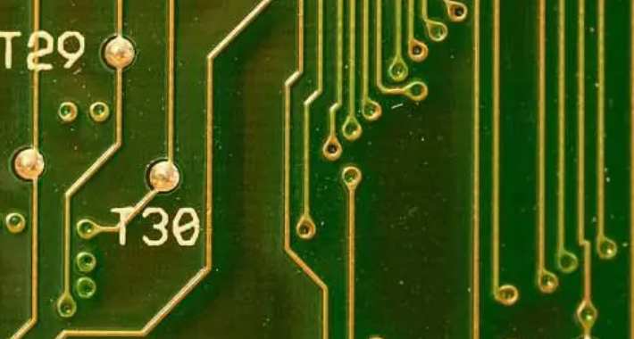
The surface of the circuit board has several processing processes: light plate (surface does not do any treatment), rosin plate, OSP (organic solder protective agent, slightly better than rosin), spray tin (lead tin, lead-free tin), gold plate, gold plate, etc., these are more visible.
We will briefly introduce the differences between gilding and sinking processes.
Gold deposition is used by chemical deposition, through the method of chemical REDOX reaction to generate a layer of coating, generally thick, is a kind of chemical nickel gold deposit method, can reach a thicker gold layer.
Gold plating is the principle of electrolysis, also known as electroplating. Other metal surface treatment is also the majority of electroplating.
In the actual product application, 90% of the gold plate is sunk gold plate, because the poor weldability of gold-plated plate is its fatal shortcoming, but also the direct cause of many companies to abandon gold-plated process!
The plating process deposited nickel gold coating with stable color, good brightness, smooth coating and good weldability on the surface of the printed circuit. It can be basically divided into four stages: pre-treatment (oil removal, micro-etching, activation, post-leaching), nickel deposition, gold deposition, and post-treatment (waste gold water washing, DI washing, drying). The thickness of the gold deposit is between 0.025 and 0.1um.
Gold is used in circuit board surface treatment, because of the strong conductivity of gold, good oxidation resistance, long life, general application such as keyboard, gold finger plate, and the basic difference between gold plate and gold plate is that gold is hard gold (wear-resistant), gold is soft gold (not wear-resistant).
1, gold and gold plating formed by the crystal structure is not the same, gold for gold thickness is much thicker than gold plating, gold plating will be golden, more yellow than gold plating (this is one of the methods to distinguish gold plating and gold plating), gold plating will be slightly white (nickel color).
2, the crystal structure formed by gold plating and gold plating is not the same, gold plating is easier to weld, will not cause poor welding. The stress of the sunk gold plate is easier to control, which is more conducive to the processing of the bunding products. At the same time, it is because the gold is softer than the gold, so the gold plate is not wear-resistant to the gold finger (the disadvantage of the gold plate).
3. There is only nickel gold on the solder plate, and the signal transmission in the skin effect is in the copper layer, which will not affect the signal.
4, gold plating is more dense crystal structure, not easy to produce oxidation.
5, with the PCB processing precision requirements more and more high, line width, spacing has been to 0.1mm below. Gilding is easy to produce gold wire short circuit. Only the solder plate has nickel gold, so it is not easy to produce gold wire short circuit.
6. Only nickel gold is deposited on the welding plate, so the welding resistance on the line is more solid with the copper layer. The work will not affect the spacing when compensating.
7, for the higher requirements of the board, the flatness requirements are better, generally the use of gold, gold will not appear after the assembly of the black pad phenomenon. The flatness and service life of the gold plate are better than that of the gold plate.
So at present, most factories have adopted the gold sinking process to produce gold plate. However, the gold plating process is more expensive than the gold plating process (higher gold content), so there are still a lot of low cost products using the gold plating process (such as remote control board, toy board).
Common methods are
Apr 02,2023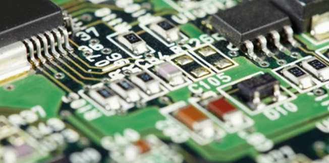


Just upload Gerber files, BOM files and design files, and the KINGFORD team will provide a complete quotation within 24h.