
Professional PCB manufacturing and assembly
Building 6, Zone 3, Yuekang Road,Bao'an District, Shenzhen, China
+86-13410863085Mon.-Sat.08:00-20:00

Why should capacitors be placed nearby in PCB design? Because it has an effective radius, it's too far away to work. An important problem of capacitance decoupling is the capacitance decoupling radius. Most of the data will mention that the capacitor should be placed as close to the chip as possible, most of the data is from the Angle of reducing the inductance of the loop to talk about this placement distance problem.
It is true that reducing inductance is an important reason, but there is another important reason that is not mentioned in most data, and that is the problem of capacitor decoupling radius.
If the capacitor is placed too far away from the chip beyond its decoupling radius, the capacitor will lose its decoupling effect.
The best way to understand the decoupling radius is to look at the phase relationship between the noise source and the capacitor compensation current.
When the chip's demand for current changes, a voltage disturbance will be generated in a small local area of the power plane. To compensate for this current (or voltage), the capacitor must first sense this voltage disturbance.
It takes a certain amount of time for the signal to travel through the medium, so there is a time delay between the occurrence of a local voltage disturbance and the perception of this disturbance by the capacitor. Similarly, a delay is required for the capacitor's compensating current to reach the disturbed region. Therefore, the phase inconsistency between the noise source and the capacitor compensation current must be caused.
A particular capacitor compensates best for noise at the same frequency as its self-resonant frequency, and we measure this phase relationship at that frequency. Set the self-resonant frequency as f and the corresponding wavelength as, and the compensation current expression can be written as:
Where, A is the current amplitude, R is the distance from the area to be compensated to the capacitor, and C is the signal propagation speed.
When the distance from the disturbance area to the capacitor is reached, the phase of the compensation current is, and it is just 180 degrees different from the phase of the noise source, that is, it is completely inverted. At this time, the compensation current no longer works, the decoupling effect fails, and the compensated energy cannot be delivered in time. In order to effectively transfer the compensating energy, the phase difference between the noise source and the compensating current should be as small as possible, preferably in phase. The closer the distance, the smaller the phase difference, the more the compensated energy is transferred, and if the distance is 0, 100 percent of the compensated energy is transferred to the disturbance region. This requires that the noise source be as close to the capacitor as possible, but much less. In practice, this distance is best controlled between, which is an empirical data.
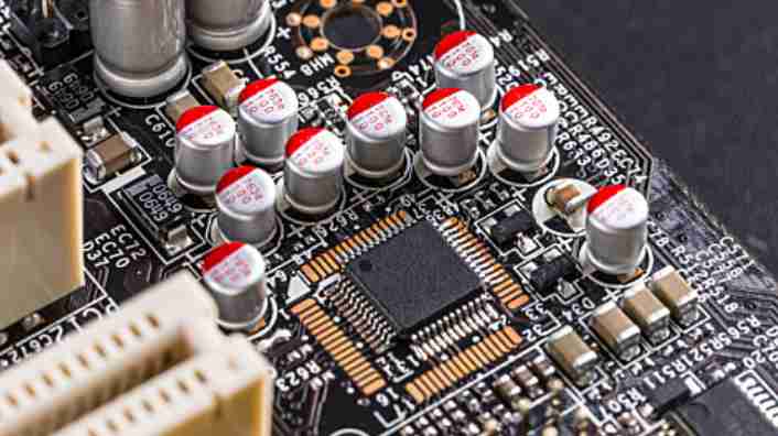
For example, if the total parasitic inductance of the 0.001uF ceramic capacitor is 1.6nH after it is installed on the circuit board, the resonant frequency is 125.8MHz and the resonant period is 7.95ps. Assuming that the signal travels at 166ps/inch on the circuit board, the wavelength is 47.9 inches. The capacitance decoupling radius is 47.9/50=0.958 inches, equal to approximately 2.4 cm.
The capacitor in this example can only compensate for the power supply noise within a range of 2.4 cm around it, i.e. its decoupling radius of 2.4 cm. Different capacitors have different resonant frequencies and different decoupling radii.
For large capacitors, because the resonant frequency is very low and the corresponding wavelength is very long, the decoupling radius is very large, which is why we do not pay much attention to the position of large capacitors on the circuit board. For small capacitors, because the decoupling radius is very small, it should be as close as possible to the chip that needs to be decoupled. This is what most data will emphasize repeatedly. Small capacitors should be placed as close to the chip as possible.

2. High-speed PCB design and wiring method to solve signal crosstalk
The unwanted noise voltage signals generated by electromagnetic fields between signals are called signal crosstalk. If the crosstalk exceeds a certain value, the system may fail to work properly. Next, Shenzhen PCB design company kingford will share with you the solution of high-speed PCB design and wiring signal crosstalk.
1. Reduce the conversion rate of signal edges where possible
In general, when designing devices, slow devices should be selected as far as possible while meeting the design specifications, and the mixed use of different kinds of signals should be avoided, because the fast transforming signal has potential crosstalk danger to the slow transforming signal.
2. Adopt shielding measures
Providing packet ground for high speed signal is an effective way to solve crosstalk problem. However, covering the ground leads to an increase in wiring, making an already limited wiring area even more crowded. In addition, ground shielding to achieve the desired purpose, ground spacing is very critical, generally less than the signal change along the length of twice. At the same time, the ground wire will also increase the signal distribution, so that the transmission line impedance increases, the signal along the slow.
3, reasonable setting of layer and wiring
Reasonable setting of wiring layer and wiring spacing, reducing the length of parallel signal, shortening the distance between signal layer and plane layer, increasing the distance between signal lines, and reducing the length of parallel signal lines (within the critical length range) can effectively reduce crosstalk.
4, set up different wiring layers
It is also a good way to solve crosstalk to set up different wiring layers for different speed signals and set plane layers reasonably.
Five, impedance matching
The magnitude of crosstalk can also be greatly reduced if the impedance of the near or far end of the transmission line matches the impedance of the transmission line.
The purpose of crosstalk analysis is to quickly find, locate and solve crosstalk problems in PCB implementation. General simulation tools and the environment of simulation analysis and PCB wiring environment are independent of each other. After the end of wiring, crosstalk analysis is carried out to obtain the crosstalk analysis report. New wiring rules are deduced and rewired, and then analyzed and corrected.
Through the simulation analysis, we can see that the actual crosstalk results are not the same, and the difference is very big. Therefore, a good tool should not only be able to analyze crosstalk, but also be able to apply crosstalk rules to wiring. In addition, general wiring tools are only driven by physical rules, and the wiring controlling crosstalk can only be restricted by setting physical rules such as line width and line spacing, as well as the maximum parallel line length. The signal integrity analysis and design tool set ICX can support the electrical rules driving wiring in the real sense. The simulation analysis and wiring can be completed in the same environment. The electrical rules and physical rules can be set during the simulation, and the signal integrity elements such as overrush and crosstalk can be calculated automatically during the wiring, and the wiring can be corrected automatically according to the calculation results. This wiring speed is fast, and really meet the actual electrical performance requirements.


Just upload Gerber files, BOM files and design files, and the KINGFORD team will provide a complete quotation within 24h.