
Professional PCB manufacturing and assembly
Building 6, Zone 3, Yuekang Road,Bao'an District, Shenzhen, China
+86-13410863085Mon.-Sat.08:00-20:00

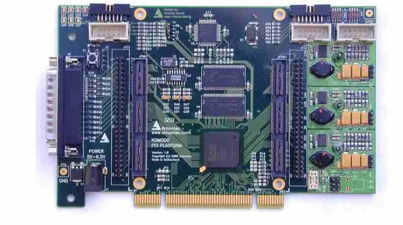
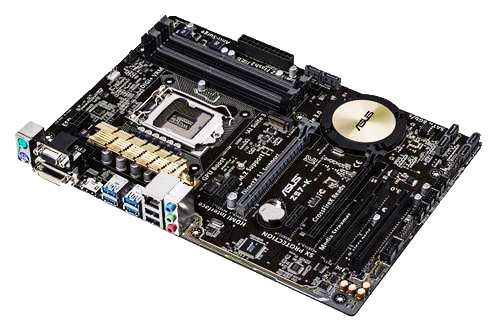
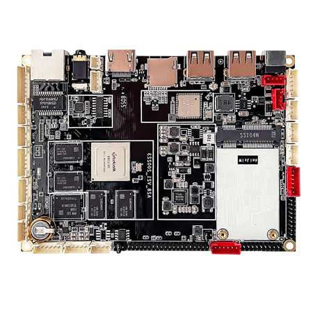
In industrial prosperity, PCB circuit boards are widely used in all kinds of electronic products. According to the different industry, PCB circuit board color and shape, size and level, data are different. Therefore, in the design of PCB circuit board needs to understand the information, otherwise it is easy to present misunderstandings. The following is the PCB circuit board in the design process of the problem summed up ten defects. The following patch manufacturer would like to tell you the characteristics of SMT processing and BGA assembly and the relevant knowledge of PCB circuit board design problems.
1. What are the design problems of PCB circuit boards
1, the processing level definition does not understand the single panel design in the TOP layer, if not clarified positive and negative, may be made out of the board installed on the device and not good welding.
2. The large area of copper foil is too close to the outer frame. The large area of copper foil should be at least 0.2mm away from the outer frame.
3. Drawing pad with filler block can pass DRC inspection when designing PCB circuit board, but the processing is not good, so the welding pad can not directly generate solder resistance data. When applying solder resistance, the filler block area will be covered by solder resistance, resulting in difficult device welding.
4, the electric formation is flower welding pad is wired because of the design of flower welding pad mode power supply, the formation and the practice of the printed board in the figure above is the opposite, all lines are isolation line, draw several groups of power supply or several ground isolation line should be heart, can not leave a gap, so that the two groups of power short circuit, can not form the connection area blockade.
5. Character misplacement of character cover pad SMD weld, which brings inconvenience to PCB on-off test and component welding. The character design is too small to form screen printing, and too large to stack the characters and make them indistinguishable.
6, appearance mount device pad is too short This is for on-off test, on the appearance mount device is too dense, the distance between the feet is quite small, the pad is also quite thin, the device test needle, must be interwoven position, such as the pad design is too short, although does not affect the device device, but will make the test needle wrong not open.
7, single-side pad aperture setting single-side pad is generally not drilled, if drilling needs to be marked, its aperture should be designed to be zero. If the values are designed so that when the borehole data is generated, the location presents the hole coordinates and presents the problem. Single - side pad should be specially marked for drilling.
8. Welding pad stacking in PCB board drilling process will cause broken bit due to repeated drilling in a place, resulting in hole damage. The two holes in the multilayer board are stacked, and the film is drawn as an isolation plate, forming a scrap.
9. In the design, there are too many filling blocks or filling blocks with extremely thin lines, resulting in loss of optical drawing data, and the optical drawing data is incomplete. Because the filling block is drawn line by line in the processing of optical drawing data, the amount of optical drawing data is quite large, which increases the difficulty of data processing.
10, graphic layer abuse in some graphic layer to do some useless connection, originally is four layers of the board but designed more than five layers of the line, so that the formation of misunderstanding. Unconventional design. PCB circuit board design should adhere to the graphic layer intact and clear.

2. What are the features of SMT processing and BGA assembly
Its technological characteristics are as follows:
1), the BGA pin (welding ball) is located under the package body, the naked eye can not directly...... The BGA(i.e., Ball GridAray) has a variety of structures, such as plastic seal BGA(P-BGA), flip BGA(F-BGA), carrier BGA(T-BGA), and ceramic BGA(C-BGA). The process features are as follows :1) The BGA pin (welding ball) is located under the package body, the naked eye can not directly observe the welding condition, must use X-ray equipment to check.
2) BGA is a humidity sensitive device. If it absorbs moisture, it is prone to deformation aggravation and bad "popcorn", so it must be confirmed whether it meets the process requirements before installation.
3), BGA is also a stress-sensitive device, the stress of the four corner solder joint is concentrated, it is easy to break under the action of mechanical stress, therefore, in the design of PCB should be placed far away from the edge of the plate and the installation of screws.
In general, BGA welding process is very good, but there are many unique welding problems, mainly related to the packaging structure of BGA, especially thin FCBGA and PBGA. Due to the layered structure of packaging, deformation will occur in the welding process, which is generally referred to as dynamic deformation. It is the main cause of many bad BGA assembly. The reason why dynamic deformation occurs in the heating process of FC-BGA is that BGA is a layered structure and the CTE difference of each layer material is relatively large. BGA encapsulation BGA welding has indicator significance in setting the temperature curve of reflow welding. Because of the large size and heat capacity of BGA, it is generally used as a key monitoring object for reflow welding temperature curve setting. The welding defect spectrum of BGA is closely related to the package structure and size. According to the common defects, it can be roughly summarized as follows:
(1) welding ball spacing < The main defects of 1.0mm BGA (or CSP) are ball and socket, non-wetting open welding, and bridging, as described in Section 4.3.
(2) welding ball spacing > Due to the dynamic deformation characteristics of 1.0mm PBGA, FBGA, etc., it is easy to occur non-wetting opening welding, non-wetting cracking, tin shrinkage fracture and other special small probability of poor welding. Generally, these welding defects are not easy to be found through routine testing, and are easy to flow to the market, with great reliability risks.
(3) Because of the large size of BGA larger than 25mmx 25mm, it is easy to cause solder joint stress fracture, pit crack and other failures.


Just upload Gerber files, BOM files and design files, and the KINGFORD team will provide a complete quotation within 24h.