
Professional PCB manufacturing and assembly
Building 6, Zone 3, Yuekang Road,Bao'an District, Shenzhen, China
+86-13410863085Mon.-Sat.08:00-20:00

What is a copy board? Copy board is also called cloning or imitation, is a product design of PCB board reverse technology research, copy board is equal to copy board, copy the circuit board on the hand, and then mass production. So how to copy the board, what do you need to prepare? Next by Chengdu Zicheng Electronic answer for you.
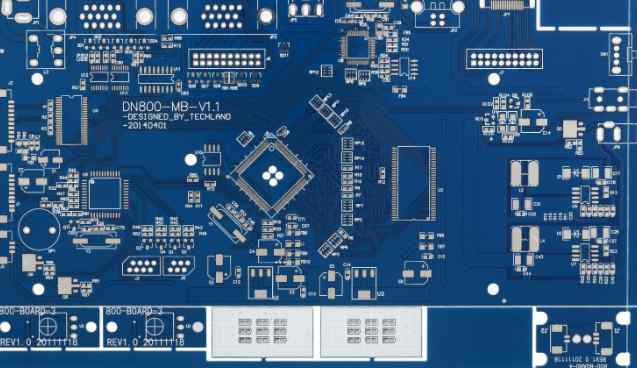
The first step is to take a PCBA circuit board and record the models, parameters and corresponding positions of all components on the pcba in notes or files. It is best to take a picture before the dissection, so as not to make mistakes during the recording process, especially the diode, the direction of the tertiary tube, the direction of the IC notch. There are a lot of BGA packages that we have to document as well.
Second, after recording all the packaged components, remove all the components and remove the tin from the PAD hole. The PCBA circuit board is cleaned with industrial alcohol and placed in a scanner that is programmed to scan with slightly higher pixels so that a clearer image of each grain and circuit and structure can be seen. Then the top and bottom layers are lightly polished with gauze paper until the copper film shines, put them in the scanner, start PHOTOSHOP, and sweep the two layers in color separately. Note that PCB must be placed horizontally and vertically in the scanner, otherwise the scanned image cannot be used.
The third step is to adjust the contrast and brightness of the canvas, so that the part with copper film is in strong contrast with the part without copper film, then turn the subdrawing to black and white, check whether the lines are clear, if not, repeat this step. If it is clear, save the picture as black and white BMP format files TOP.BMP and BOT.BMP. If there is any problem with the picture, you can use photo shop to repair and correct it.
The fourth step is to convert the two BMP files into protel files respectively, and transfer two layers into PROTEL. For example, the position of PAD that has passed two layers is basically identical with that of ⅥA, which indicates that the previous steps have been done well. If there is any deviation, repeat the third step.
Step 5, convert the BMP of the TOP layer to the TOP.PCB, be careful to convert to the SILK layer, which is the yellow layer. Then you trace the line on the TOP layer and place the device according to the drawing of step 2. Delete the SILK layer when you are done. Repeat until all layers are drawn.
In the sixth step, TOP.PCB and BOT.PCB are transferred into PROTEL, and it is OK to combine into a figure.
Step 7: Use a laser printer to print the TOPLAYER and BOTTOM LAYER onto the transparent film (1:1 ratio), place the film on the PCB, compare and see if it's wrong, if it's right, you're done.
A copy of the original board was created, but it was only half done. But also to test, test copy board electronic technology performance is the same as the original board. If it's one, it's really done.
In addition, there is skin effect in the RF condition. Unlike DC, where current flows throughout the conductor, current flows over the surface at high frequencies. As a result, the AC resistance at high frequencies is greater than the DC resistance.
Another problem in high frequency circuits is the effect of electromagnetic radiation. As the frequency increases, the circuit becomes a radiator when the wavelength is comparable to the circuit size of 12. At this time, there will be various coupling effects between circuits, circuits and the external environment, which leads to a lot of interference problems. These problems are often irrelevant at low frequencies.
With the development of communication technology, the frequency used in communication equipment is increasing day by day. Radio frequency (RF) and microwave (MW) circuits are widely used in communication systems. The design field of high frequency circuit has been paid special attention by the industry. The carrier frequency of microwave radio frequency identification system (RFID) is in the frequency range of 915MHz and 2450MHz; The Global Positioning system (GPS) carrier frequency is in the frequency range of 1227.60MHz and 1575.42MHz; The RF circuit in the personal communication system operates at 1.9GHz and can be integrated into the increasingly small personal communication terminals; The C band satellite broadcast communication system includes 4GHz uplink and 6GHz downlink. These circuits typically operate at frequencies above 1GHz, and with the development of communication technology, this trend will continue. However, dealing with such high frequency circuits requires not only special equipment and devices, but also theoretical knowledge and practical experience not used in DC and low frequency circuits.
Three. Applications of radio frequency circuits

RF(Radio Frequency) technology is widely used in many fields, such as: television, radio, mobile phone, radar, automatic identification system and so on. The special word RFID(radio frequency identification) refers to the application of radio frequency identification signals to identify the target. Applications of RFID include:
ETC(electronic toll collection)
Railway rolling stock identification and tracking
Container identification
Identification, authentication and tracking of valuables
Target management for retail, healthcare, logistics, etc
Access control
Animal identification and tracking
Automatic locking of vehicle (anti-theft)


Just upload Gerber files, BOM files and design files, and the KINGFORD team will provide a complete quotation within 24h.