
Professional PCB manufacturing and assembly
Building 6, Zone 3, Yuekang Road,Bao'an District, Shenzhen, China
+86-13410863085Mon.-Sat.08:00-20:00

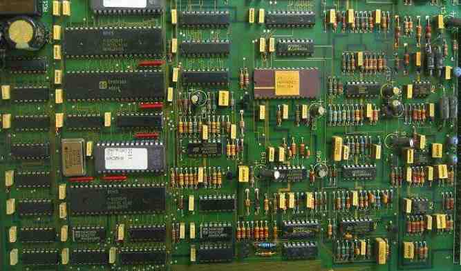
PCB board has double-sided PCB, four-layer PCB, six-layer PCB, eight-layer PCB, etc. At present, there are more than 100 layers of PCB, then why do people have "PCB multilayer board why are even layers?" What about this question? Relatively speaking, even layer PCB does have more than odd layer PCB.
PCB board has double-sided PCB, four-layer PCB, six-layer PCB, eight-layer PCB, etc. At present, there are more than 100 layers of PCB, then why do people have "PCB multilayer board why are even layers?" What about this question? Relatively speaking, even layer PCB does have more than odd layer PCB.
1, the balance structure to avoid bending
The reason for not designing PCBS with odd layers is that odd layers are easy to bend. When the PCB is cooled after the multilayer circuit bonding process, the different lamination tension between the core structure and the foil structure can cause the PCB to bend when cooled. As the board thickness increases, the risk of bending becomes greater for composite PCBS with two different structures. The key to eliminate circuit board bending is to use balanced layering. Although PCBS with a certain degree of bending meet the specification requirements, subsequent processing efficiency will be reduced, resulting in increased costs. Because assembly requires special equipment and technology, the accuracy of component placement is reduced, so the quality will be damaged.
To put it in a more understandable way: In PCB process, four-layer board is easier to control than three-layer board, mainly in the aspect of symmetry, the warpage degree of four-layer board can be controlled below 0.7% (IPC600 standard), but when the size of three-layer board is large, the warpage degree will exceed this standard, which will affect the reliability of SMT and the whole product, so generally designers do not design odd layer board , even if the odd layer to achieve the function, will also be designed as false even layer, that is, 5 layers design into 6 layers,7 layers design into 8 layers.
2. Low cost
Because there is one less layer of medium and coating foil, the cost of odd-numbered PCB board raw materials is slightly lower than that of even-numbered PCB board. But the processing cost of odd layer PCB is obviously higher than that of even layer PCB. The inner layer has the same processing cost, but the foil/core structure significantly increases the processing cost of the outer layer.
Odd layer PCB needs to add non - standard laminated core layer bonding technology on the basis of nuclear structure technology. Compared with the nuclear structure, the production efficiency of the plant adding foil outside the nuclear structure will decrease. Prior to laminating, the outer core requires additional processing, which increases the risk of scratches and etching errors on the outer layer.
For the above reasons,PCB multilayer boards are mostly designed with even layers, and odd layers are less.
So how to reduce the cost and balance the stacking of odd-layer PCBS?
What if there are an odd number of PCBS in the design? The following methods can be used to balance layering, reduce PCB production costs and avoid PCB bending.
1) Add an additional power layer. This method can be used if the PCB is designed with odd power layers and even signal layers. An easy way to do this is to add a layer in the middle of the stack without changing the other Settings. Route an odd number of PCB layers first, then duplicate layers in the middle and label the remaining layers. This is the same electrical property as the coating of thickened layers.
2) A signal layer and use. This method can be used if the PCB is designed with even power layers and odd signal layers. The additional layer does not increase the cost, but can shorten the lead time and improve PCB quality.
3) Add a blank signal layer near the PCB stack. This method reduces layering unbalance and improves PCB quality. The odd-numbered layers are routed, and a blank signal layer is added to mark the remaining layers. In microwave circuits and mixed media (media with different permittivity) circuit types are used.
When testing PCB board, we should pay attention to the following 9 tips to ensure the quality of the product.
1.PCB detection
It is strictly prohibited to test PCB board by using grounded test equipment to contact the TV, audio, video and other equipment on the baseboard that is live without isolating transformer
It is strictly prohibited to directly test TV, audio, video and other equipment without power isolation transformer with the instrument whose shell has been grounded. Although the general radio recorder has a power transformer, when exposed to the more special especially large output power or the nature of the power supply is not very familiar with the television or audio equipment, first of all to make clear whether the chassis of the machine is live, otherwise it is easy to and floor live TV, audio and other equipment caused by short circuit, ripple integrated circuit, resulting in further expansion of the fault.
2. Pay attention to the insulation performance of electric soldering iron when detecting PCB board
Do not allow the use of electric soldering iron welding, to confirm that the iron is not charged, the shell of the iron ground. MOS circuit should be more careful, can use 6~8V low voltage circuit iron is safer.

3. Understand the working principle of the integrated circuit and its related circuits before testing the PCB board
Before checking and repairing integrated circuit, we should be familiar with the function, internal circuit, main electrical parameters, the role of each pin, and the normal voltage, waveform and components of the pin circuit. If these conditions are in place, analysis and inspection are much easier.
4. Do not cause short circuit between pins when testing PCB board
When measuring voltage or testing waveform with oscilloscope probe, the stylus or probe should not be short-circuited between the pins of integrated circuit due to sliding, so the measurement should be carried out on the printed circuit directly connected with the pins. Any momentary short circuit can easily damage the IC, and extra care should be taken when testing CMOS integrated circuits in flat packages.
5. The PCB board test instrument should have high internal resistance
When measuring the DC voltage of integrated circuit pins, use a multimeter with an internal resistance greater than 20 kω /V. Otherwise, there will be a large measurement error for some pins.
6. Pay attention to the heat dissipation of power integrated circuit when detecting PCB board
The heat dissipation of the power integrated circuit should be good. It is not allowed to work in a high power state without a radiator.
7. Test the PCB board leads properly
If you need to add components to replace the damaged part of the integrated circuit, small components should be selected, and wiring should be reasonable to avoid unnecessary parasitic coupling, especially to deal with the audio power amplifier integrated circuit and the pre-amplifier circuit between the ground terminal.
8. Check PCB board to ensure welding quality
Welding is really solid, the accumulation of solder, porosity is easy to cause virtual welding. Welding time is generally not more than 3 seconds, the power of the iron should be about 25W internal heat. The soldered integrated circuit should be carefully checked, and the ohmmeter should be used to measure whether there is short circuit between the pins to confirm that there is no solder adhesion phenomenon before switching on the power supply.
9. Detection PCB board do not easily determine the damage of integrated circuit
Do not easily judge the integrated circuit has been damaged, because the vast majority of integrated circuits are direct coupling, once a circuit is abnormal, may lead to multiple voltage changes, and these changes are not necessarily caused by the damage of the integrated circuit. In addition, in some cases, when the pin voltage is consistent with or close to the normal value, it may not be able to show that the integrated circuit is good, because some soft faults will not cause changes in DC voltage.
Super - complete pcb failure analysis technology
Feb 09,2023


Just upload Gerber files, BOM files and design files, and the KINGFORD team will provide a complete quotation within 24h.