
Professional PCB manufacturing and assembly
Building 6, Zone 3, Yuekang Road,Bao'an District, Shenzhen, China
+86-13410863085Mon.-Sat.08:00-20:00

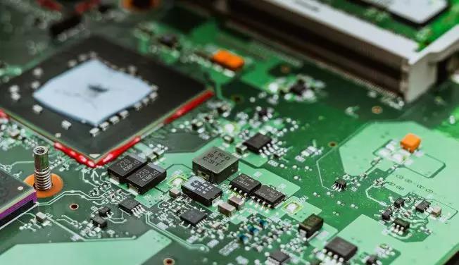
With the continuous progress of science and technology, the quality control of PCB circuit boards is becoming more and more strict, and then the development and upgrading of PCB surface treatment technology is becoming more and more urgent.
Why surface treatment
Since the copper layer on the PCB is easily oxidized, the resulting copper oxide layer can seriously degrade the weld quality, thereby reducing the reliability and effectiveness of the final product. In order to avoid this, PCB surface treatment is required. Some materials will say surface molding, the board factory process will be differentiated, it is believed that the outermost layer of PCB board and on the copper, play the role of copper "coating".
Historical evolution of common surface treatments:
The surface treatment process uses a flux to weld components on the copper surface from the beginning, and when the product is required in large quantities, tin-lead plating is used. Hot air solder smoothing (HASL) begins to appear when PCB boards are coated with solder resistance. With the increase of wiring density, organic solderability protective film (OSP) appeared. For clean assembly operations, the ENIG process was widely used, and later came to be environmentally lead-free
Chemical precipitation of silver, chemical precipitation of tin, chemical nickel palladium, chemical nickel silver (ENIAg), etc.
There are two main types of surface treatment processes: metallic and organic.
(1) HASL, ENIG/ENEPIG, gold sinking and tin sinking belong to metal surface forming,
(2) OSP belongs to organic surface forming.
1, mechanical anti-oxidation (OSP)
OSP is printed circuit board (PCB) copper foil surface treatment in line with the RoHS directive requirements of a process.
OSP is an Organic Solderability Preservatives. To put it simply, OSP is chemically growing an organic skin film on the surface of clean bare copper.
This layer of film has anti-oxidation, heat shock, moisture resistance, to protect the surface of copper in the normal environment no longer continue to rust (oxidation or vulcanization, etc.); However, in the subsequent welding high temperature, this protective film must be easily removed by the flux quickly, so that the exposed clean copper surface can be immediately combined with the molten solder into a solid solder spot in a very short time, to ensure the solderability of PCB surface copper. Unlike other surface treatments, OSP is limited to solderability protection.
This large organic molecule is dissolved in a solution of water and organic acid. The PCB is immersed in the solution, and the exposed copper forms chemical bonds with these molecules, forming an Op-copper composite layer on the copper surface. The thickness can be 0.10~0.60um.
The downside is that once the OSP coating is too thick, it can affect welding. There is no way to check that the copper is fully protected. It is also important to note that PCbas using conventional wave soldering and selective wave soldering processes are not allowed to use OSP surface treatment.
2. Hot Air Leveling (HASL)
Hot air leveling, also known as hot air solder leveling (commonly known as tin spray), is a process of coating molten tin (lead) solder on the surface of PCB and heating compressed air leveling (blowing), so that it forms a layer of copper oxidation resistance, and can provide good solderability of the coating.
(1) Lead spray tin
The so-called lead spray tin refers to the tin according to a certain proportion, modulated, lead will improve the activity of tin line in the welding process, lead tin line is relatively better than lead-free tin line, but lead is toxic, lead in the lead is harmful to human health; The eutectic temperature with lead is lower than that without lead. How much depends on the composition of lead-free alloy ah, like SNAGCU eutectic 217 degrees, welding temperature is eutectic temperature plus 30 to 50 degrees. Lead eutectic is 183 degrees. Mechanical strength and brightness are better with lead than without lead. Therefore, lead tin is not environmentally friendly, and the world advocates a certain amount of environmental protection. Thus, lead-free spray tin was born.
(2) lead-free tin spray
Lead-free tin is a kind of environmental protection process, it is very small harm to human health, is also advocated at the present stage of a process, lead-free tin for lead content is not more than 0.5, lead-free tin melting point is high, so that the welding point is firm. Essentially lead spray tin and lead - free spray tin is a process. It's just the purity of the lead is different. And lead-free tin is more environmentally friendly and safer for the human body and the environment. It is also a development trend in the future. It is recommended that you use it.
3. Sink gold
Gold plating is a thick layer of good electrical nickel gold alloy on the copper surface, which can protect the PCB for a long time; In addition, it has environmental tolerance that other surface treatment processes do not have. Sinking gold also prevents copper from dissolving, which would help lead-free assembly.
Its advantages are not easy to oxidize, can be stored for a long time, smooth surface, suitable for welding fine clearance pin and small solder joint components. Preferred PCB board with keys (such as mobile phone board). It can be repeated multiple times without much loss of weldability. Can be used as the base material for COB (Chip On Board) wire.
Its disadvantage is that the cost is higher, the welding strength is poor, because the use of nickel plating process, easy to have the problem of black disk. The nickel layer oxidizes over time and does not have long-term reliability.
4. Sink silver
Between OSP and electroless nickel plating/gold leaching, the process is simple and fast. Exposure to heat, humidity and pollution will still provide excellent electrical properties and maintain good weldability, but will tarnish. Because there is no nickel underneath the silver layer, sunken silver does not have all the good physical strength of electroless nickel/gold plating.
Copper on chemically precipitated silver (IMS) PCBS needs to be cleaned separately and pre-treated with micro-etching, and Javani displacement is performed between inert copper and more inert silver in the silver solution.
The resistance of chemical silver deposition to creeping corrosion is relatively poor. Creeping corrosion refers to the phenomenon that PCB or PCBA is exposed to moisture and other gases and slowly corrodes crystals within a certain period of time, which may cause short circuit or open circuit problems.
5. Sinking tin
PCB tin deposition process is specially designed to facilitate SMT and chip packaging. It is a new green process to replace Pb-Sn alloy coating process. It has been widely used in the surface treatment of electronic products (such as circuit boards, electronic devices), hardware, ornaments and so on.
Chemical precipitation of tin is similar to chemical precipitation of silver, but tin is an amphoteric metal, and can react with acids and bases, so after deposition, to avoid contact with strong acids and bases.

6. Nickel gold
Electroless nickel/gold Leaching (ENIG) and Electroless nickel palladium Plating (ENEPIG)
ENIG(Electroless Nickel Immersion Gold), consisting of a thin layer of electroless nickel plating and gold immersion, involves a CU/Ni/Au three-layer metal structure. The process mainly includes: activated copper, electroless nickel plating, chemical gold leaching. It protects nickel from oxidation. Gold is ideal for PCB coating because it does not form oxides, is less affected by temperature and storage conditions, and is easy to solder. However, if the gold content exceeds 3% of the solder mass, it will make the solder joint brittle, so the maximum thickness of the gold layer in the welding is 0.3um.
Gold melts into copper very quickly. In order to prevent gold from fusing with copper and eventually exposing the copper to oxidation, resulting in welding problems, nickel plating is used to separate the gold and copper. Nickel plating/gold leaching is not an electrochemical process, just allowing nickel as an oxidant to be reduced by phosphorus and eventually deposited. Typically, 3 to 5um of nickel is sunk first, and 0.05 to 0.15um of gold is added to the nickel to prevent oxidation.
ENEPIG is (Electroless Nickel Electroless Palladium Immersion Gold).
It involves CU/Ni/PD/Au four-layer metal structure. The difference between ENEPIG and ENIG is that there is an extra layer of palladium between nickel and gold. In the deposition reaction of replacement gold, the electroless palladium layer will protect the nickel layer and prevent it from being excessively corroded by replacement gold. Palladium is fully prepared for gold leaching while preventing the corrosion phenomenon caused by replacement reaction.
The difference between nickel corrosion phenomena process:
ENIG(chemical nickel gold) is mainly used for the surface treatment of circuit boards to prevent oxidation or corrosion of copper on the surface of circuit boards, and for welding and contact applications, such as gold fingers on memory strips.
ENEPIG(nickel palladium leaching) is mainly used for packaging substrate surface treatment. In the process of nickel palladium leaching, accurate deposition thickness and gold layer uniformity can be obtained by controlling the electroless palladium plating and gold leaching on the nickel layer, so as to achieve good contact surface.
7. PCB board mixed surface treatment technology
Choose two or more kinds of surface treatment methods for surface treatment, common forms are: nickel gold + anti-oxidation, nickel plating gold + nickel plating gold, nickel plating gold + hot air leveling, nickel plating gold + hot air leveling, lead-free spray tin + gold finger.
How does PCB design avoid crosstalk
Feb 06,2023


Just upload Gerber files, BOM files and design files, and the KINGFORD team will provide a complete quotation within 24h.