
Professional PCB manufacturing and assembly
Building 6, Zone 3, Yuekang Road,Bao'an District, Shenzhen, China
+86-13410863085Mon.-Sat.08:00-20:00

Share and explain how to build multilayer PCB stack in PCB design
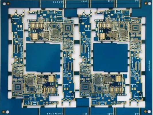
There are more than two layers in the stack of multilayer PCBs. Stacking is one of the most important aspects of design. It describes how layers are arranged on a multilayer board. Properly stacked boards will reduce electromagnetic radiation, crosstalk, and improve signal integrity.
What is a PCB stack?
Stacking describes the construction of multilayer plates in sequence. It provides vital information, such as the material thickness and copper weight required to make PCBs. Stacking is also called stacking. The stack also provides details on the routing width of different controlled impedance routes (e.g., 50ohms, 100ohms differential).
What are the different layers in the board?
The stack is mainly composed of metal foil, prepreg and copper clad laminate (core).
Metal foil: Copper is the most commonly used metal foil in PCB architecture.
Prepreg: It is a kind of interwoven glass cloth impregnated with epoxy resin. Resin is semi cured.
Copper clad laminate: The copper clad laminate is made by bonding a single layer or multiple layers of prepreg with the top and bottom copper foils. This is also called the core.
Power layer and ground plane in PCB stack
The power plane is the copper layer connected to the power supply. It is usually designated as VCC in PCB design. The main function of the power plane is to provide a stable power supply for the PCB. On a multilayer board, if a component needs to draw power, it is simply connected to the via that contacts the power layer. Similarly, the ground plane is a flat copper layer connected to the common ground point in the PCB.
Advantages of using power/ground plane
The power and ground pins of the component can be easily connected to the power and ground plane.
It provides a clear current return path, especially for high-speed signals. This in turn reduces EMI (electromagnetic interference).
The power plane has greater current carrying capacity than the wiring. This also reduces the operating temperature of the PCB.
What is PCB coating?
Laminating is the process of bonding prepreg and copper foil to the inner layer of the base PCB by placing the lamination under extreme temperature and pressure. Temperature and pressure values are mentioned in the data sheet of the selected PCB material.
What is the standard plate thickness?
The thickness of PCB mainly depends on such factors as copper thickness, materials used, layers and operating environment. The standard thickness of a regular plate is approximately 62 mils (1.57 mm). Nowadays, with the increasing weight and number of copper layers in various applications, PCB becomes more and more complex. Therefore, PCB tends to become thicker. According to customer requirements, the manufacturer is now manufacturing PCBs with two new standard thicknesses, 93 mils (2.36 mm) and 125 mils (3.17 mm) (150% and 200% of the old standard thickness, respectively).
Why do I need multiple layers in PCB?
In this modern era, electronic equipment has become more and more complex and composed of more components and circuits. It is a tedious task to include complex circuits in a single layer PCB. You can solve this problem by adding layers to the stack.
Let's take a look at some of the advantages of multilayer boards:
They can accommodate the complex circuits required by modern electronic equipment.
Having more layers means that the board is thicker than a single sided PCB and therefore more durable.
Multilayer boards require more planning and intensive production processes, so their quality is higher than other types of boards.
Using multiple PCB components will require multiple connection points. On the other hand, multilayer boards are designed to work with a single connection point, simplifying the design of electronic equipment and further reducing weight.
How to make multilayer circuit board?
Step 1: Inner core selection
A stack represents a material used to make a multilayer circuit board. The meeting provides the following information:
Thickness and weight of copper
Type of epoxy glass used
Panel size
Step 2: Cleaning
The inner layer shall be chemically/mechanically cleaned or both to remove contaminants from the copper surface.
Step 3: Inner layer imaging
The imaging material is placed on the copper surface. It covers the required copper circuit and exposes excess copper.
Step 4: Etch stripping
The inner layer is chemically etched to remove excess copper. The photoresist is then stripped to expose the copper circuit.
Step 5: Automatic optical inspection
Perform automatic optical inspection to detect defects that cannot be detected by human eyes (short circuit/opening in inner layer).
Step 6: Oxide treatment
Before laminating, the exposed copper circuit on the inner layer must be treated to improve the adhesion. The improved adhesion can also improve the structural strength and the reliability of the integral board.
Step 7: lay up
Repeat steps 1 to 6 for all inner layers. For example, these steps will be performed for layers 2, 3, and 4, 5.
Step 8: Film covering
In this step, the lamination is pressed and heated in a vacuum chamber. The lamination process begins with the application of vacuum to remove all residual air and gas. After that, heat and pressure are applied to the lamination to make the resin in the prepreg molecular bond.
Step 9: Drilling
After the lamination process, the laminate is loaded onto the exit material plate on the drilling machine. Drill holes on the PCB to form through holes and through holes. The export material reduces the formation of burrs. Burrs are copper protrusions formed when the drill shaft passes through the plate. To learn about the
Step 10: Deburring and Decontamination
In this step, the copper burrs formed during drilling are removed. It also removes all fingerprints from the copper surface. Decontamination is the process of removing molten resin during drilling. Immerse the PCB panel in a series of chemical solutions, and then immerse it in potassium permanganate or concentrated sulfuric acid to remove epoxy resin stains. It can also be decontaminated by plasma treatment.
Step 11: Drilling copper plating
After deburring and decontamination, the drill holes shall be copper plated by chemical methods.
HDI board stacking
High density interconnection, or HDI, is a higher wiring density per unit area of printed circuit boards than traditional printed circuit boards. In general, HDI PCB includes micro holes, blind holes, buried holes, laminations and high signal performance considerations.
Sequential lamination
PCB is manufactured by laminating epoxy prepreg glass fiber board between copper layers. These layers are laminated together under high temperature and pressure. Sequential stacking is the process of inserting a dielectric between a copper layer and a stack subset (stack).
6-layer stack with micropores
The buried through-hole can be built into the HDI board using the sequential lamination process. The first step is to fabricate layers connected by buried vias (layers 2, 3, 4, and 4 in a given layer). Next, the outer layers (layers 1 and 6) are laminated and micro through-hole is drilled.
Now let's assume that the design requires a connection between L1 and L3. L6 and L4. The best way to achieve this design is to use staggered or stacked vias.
Staggered through holes essentially mean fewer process steps. We do not need to fill the laser drilled hole with copper, because the second laser drill will not fall on the first laser drill. Filling or electroplating of micro through-hole is usually carried out in a special electroplating tank designed with chemicals. It electroplating the micro holes drilled by laser from the bottom of the through hole to the top of the through hole until it completely fills the hole. Electroplating laser drilling micro through-hole will increase process time and cost.
Terminology for HDI stacking
HDI stack architecture can be divided into stack categories according to the number of micro pore layers and the number of internal layers between micro pores. These categories are determined by the formula XNX, where x is the number of layers of micropores and N is the number of inner layers between micropores.
PCB stacking suggestions
The cost of the circuit board needs to be optimized as low as possible. To this end, the following points need to be considered:
Each layer of sequential lamination requires additional time and process. As a result, more sequential lamination in quantity increases costs and delivery schedules. It is best to limit the number of consecutive layers to 3 or less.
Stacked through holes need to be filled after each successive layer. This requires more manufacturing process steps and time. Therefore, if stacking through holes can be avoided, staggered through holes are recommended.
When the manufacturer is required to stack, please clearly mention the requirements for mechanical burial of vias between layers and for staggered and buried vias.
Some materials are not suitable for sequential lamination. The suitability of sequential laminates shall be verified by the manufacturer.
A successful PCB design depends largely on stacking. The carefully designed stack allows the designer to optimize the design for better signal integrity and reduced crosstalk and EMI. In this paper, we introduce the basic insights of PCB stack manufacturing steps. In the comments section, let us know if you want to know more about specific topics. The PCB processing factory explains how to build multilayer PCB stack in PCB design. Stacking is one of the most important aspects in the design.
Analysis of common sense in PCB design
Dec 07,2022


Just upload Gerber files, BOM files and design files, and the KINGFORD team will provide a complete quotation within 24h.