
Professional PCB manufacturing and assembly
Building 6, Zone 3, Yuekang Road,Bao'an District, Shenzhen, China
+86-13410863085Mon.-Sat.08:00-20:00

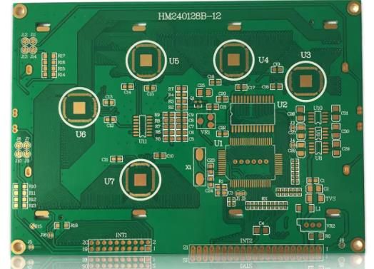
PCB factory explains why PCB layout preparation is important
Nowadays, portable, wearable and adaptive technologies have become the norm. As a result, PCBs need to be smaller in size, but can still perform increasingly complex functions with smaller components. As PCB designers, we are constantly challenged to meet these requirements by using the most effective component placement and PCB layout without affecting their electronic functions.
As a result, PCB layout becomes a key part of any design.
Start by thinking about how to end
Prioritizing the most important requirements can help simplify the design process by identifying design constraints. The size and location of key elements (including minimum and maximum tolerances), required components, and electrical requirements, including impedance factor and power requirements, are all combined to create a set of initial constraints for PCB design.
It is also a good habit to create and save collections of similar constraints and templates for subsequent designs or projects. Providing time proven templates can simplify the design of new boards or upgrade existing PCBs. Once the constraints are set and understood, it will make the details less error prone, thus saving time and money.
The circuit board layout technology may include strategies such as embedding devices in the inner layer of a PCB to reduce the size of the circuit board. The evaluation must be carried out with the manufacturer to verify that these functions can be met in actual manufacturing.
Errors or insufficient planning in the layout specification of PCB design can lead to a variety of problems:
• Finished products that do not conform to regulations or design
• Component and circuit paths that conflict with other circuit board components due to factors such as electromagnetic interference, current, routing width, component size, and physical limitations of the circuit board, may have quality or functional problems.
• Circuit boards may not be manufactured in full compliance with regulations, resulting in repeated decisions between designers and manufacturers. This increases delivery time and costs.
• Worst case – the engineer returns to the "drawing board" to rework the design for manufacturability.
Manufacturing design
Obviously, the main goal is to create a circuit board that can be manufactured efficiently and economically. Understanding the manufacturing process is a real benefit because it enables engineers to understand how manufacturing methodologies will react to their design. Layered and double-sided laminate or double-sided component placement designs can make layout more critical in DFM. IPC CID training can also help guide some of these layout decisions.
DFM software is an effective tool for PCB designers before prototype creation. These tools analyze the designer's documentation and evaluate any problems or omissions related to manufacturing. Combining PCB design tools with DFM applications is the best solution for designing the highest quality PCB with functionality and cost-effectiveness.
It is also important to work with the manufacturer, who provides extensive support for all technical aspects of PCB orders, including detailed review of submitted designs using CAM tools. PCB processing and PCB assembly plants explain that these requirements can be met by using the most effective component placement and PCB layout without affecting their electronic functions.


Just upload Gerber files, BOM files and design files, and the KINGFORD team will provide a complete quotation within 24h.