
Professional PCB manufacturing and assembly
Building 6, Zone 3, Yuekang Road,Bao'an District, Shenzhen, China
+86-13410863085Mon.-Sat.08:00-20:00

The wiring of high frequency circuit board can be divided into automatic and manual. To meet the requirements of PCB design, the wiring of high frequency circuit board must be carried out. Normally, manual wiring is required for wiring. After manual wiring, check these signal lines and then perform automatic PCB wiring.
What problems should we pay attention to when wiring high-frequency circuit boards? The following two points should be noted:
The routing of high-frequency circuit board adopts full straight line. In special cases, 45 degree broken line or arc curve is used to complete the routing. This is mainly to prevent the signal lines of high-frequency circuit board from circuitous collision with each other.
It should also be noted that the signal line of the high-frequency circuit board should not be too long, and the wiring length of the high-frequency signal should be reasonably selected to reduce the signal loss.
Fixed components should be placed first when placing components. If there are special and large components, you can choose to place them at this time. When placing components, you should consider the requirements of components. As mentioned earlier, the wiring length must be short, and the placement of components on high-frequency circuit boards must be compact, so as to prevent cross interference between signal lines
How to carry out PCB proofing
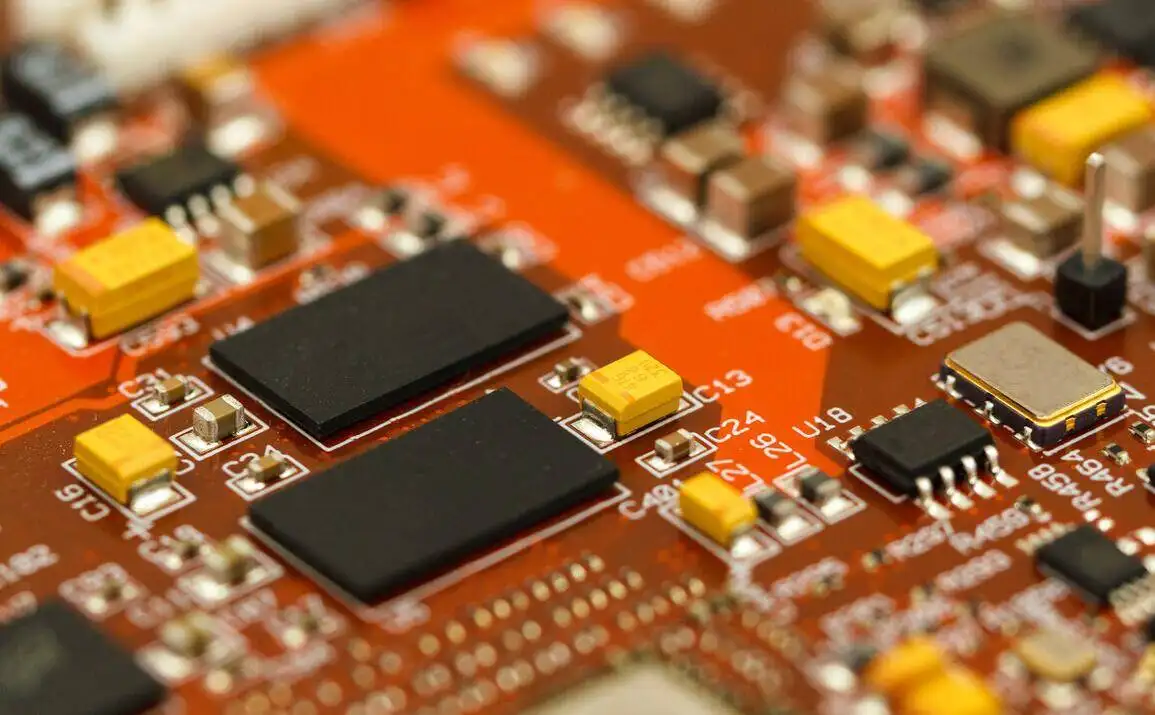
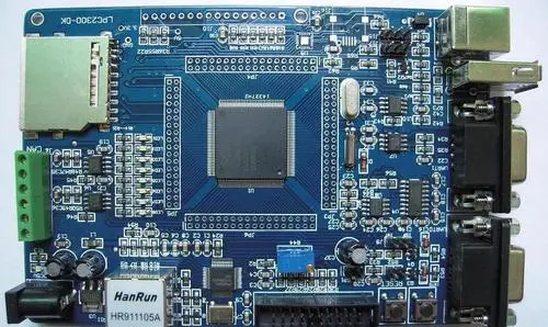
Circuit board proofing refers to small batch production before batch production of circuit boards. First, engineers design the circuit. The factory conducts small batch production according to the circuit design, which is called pcb proofing. The number of pcb proofing is not specific, but is based on the project side
Pcb proofing
Precautions for PCB proofing:
Quantity: The first one is to specify the production quantity of PCB.
Materials: To explain what kind of PCB materials are needed, FR4 is the most common one at present, and the main material is epoxy resin glass fiber cloth.
Board layer: The number of layers you make PCB should be stated. (The production layers of pcb boards are different, and the prices are also different. Generally, the higher the layers are, the higher the price will be. However, the process of pcb board proofing is much the same.)
Copper thickness: Generally, the copper thickness is calculated scientifically according to the current of PCB circuit. Generally, the thicker the copper, the better, but the cost and price will also be higher, so a reasonable balance is required.
Pcb proofing
Do you know about PCB proofing?
Soldering resistance color: There are many colors for welding resistance, such as red oil plate, butter plate, blue oil plate, etc., which can be selected according to the company's requirements. Generally, green ink is most commonly used.
Pcb proofing
Do you know about PCB proofing?
Whether the vias are covered with resistance welding: resistance welding is to insulate the vias, otherwise the vias will not be insulated.
Surface technology: there are tin spraying, gold deposition, gold plating, OSP, silver deposition, etc. Different surface technologies have their own advantages and prices will be different.
Pcb proofing
Do you know about PCB proofing?
Precautions for PCB proofing
1. Do a good job of signal integrity PCB layout, reduce noise and improve PCB stability.
2. Carry out a comprehensive electrical inspection to improve the electrical performance of the PCB board.
3. Specially confirm the device packaging to avoid the failure of proofing due to packaging errors.
4. Carefully select the proofing quantity to effectively control the cost.
Describe the doubts related to PCB design
Dec 06,2022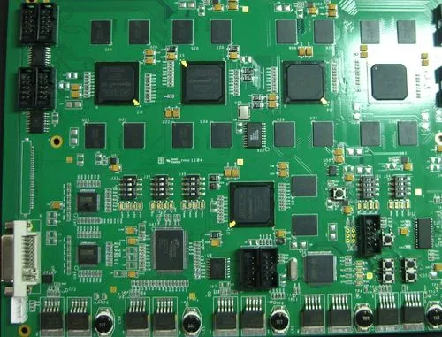


Just upload Gerber files, BOM files and design files, and the KINGFORD team will provide a complete quotation within 24h.