
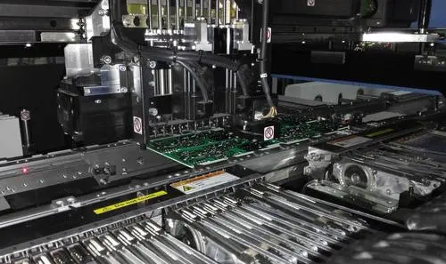
Professional PCB manufacturing and assembly
Building 6, Zone 3, Yuekang Road,Bao'an District, Shenzhen, China
+86-13410863085Mon.-Sat.08:00-20:00

The etching of pcb board is to etch the unused parts in the circuit design, which is an essential part of the whole PCB design. Let's briefly talk about the process etching.
Etching, stripping and etching machine of pcb board:
Etching methods can be divided into dipping, splash, spray and rotary spray. The operator must have a full understanding of the maintenance, control and adjustment of the circuit board etching machine to eliminate the problem. The general attention also includes the following four items:
(1) Air extraction speed: generally, it is appropriate to maintain a slight negative pressure, so that a large amount of ammonia will not escape, which will hinder the health of operators, and keep the pH within a certain range. In addition, an appropriate amount of air will enter the spraying area to supply oxygen for cuprous oxidation and maintain the normal reaction. Excessive air extraction will quickly reduce the concentration of free ammonia, reduce the pH, slow the etching rate, and reduce the etching energy. Insufficient air exhaust, ammonia escaping out of the machine, the etching solution will be anoxic, and the effective copper, namely Cu2+, will also slow down the etching rate
(2) Addition and discharge system: discharge first and then discharge, and discharge at the same time. A part of it enters from the cleaning tank (reducing the copper content in the cleaning wastewater). The effect is different. For the etching of fine lines, how to keep the parameters of the etching solution within the specified range when discharging. When the outdoor temperature is very cold in winter, it is better to maintain the sub liquid temperature above 10 ° C. On the one hand, ammonium chloride will not crystallize, and on the other hand, the bath liquid temperature will not change greatly. Circuit board plants will generally control it well.
(3) Nozzle and spraying pressure: the upper and lower pressure should be adjusted properly, and the spray overlap uniformity of nozzle angle should be tested to determine the optimal spraying pressure.
(4) Conveying rate: it shall be adjusted from time to time depending on pH, copper content and real specific gravity. Generally, 99% of copper has been etched when passing through 3M spraying area. Fine line etching: the so-called thin line refers to the circuit with line width and line space no more than 5mil. There is also a line width of 5? 8mil is called fine PCB circuit. Those below 5mil are called super fine lines.
With the etching of fine lines, PCB substrates are mostly thin copper (]/2oz) or ultra-thin copper (: 3/8oz, 1/. 4oz or l/8oz). High speed copper thickening is used for overall copper plating to make the thickness uniform. If full electric forging is adopted, it is better to use double hangers and hang one piece separately to achieve uniformity of current density. The anode distribution and the throwing power of copper plating solution have great influence. If alkaline etching solution is used for etching, the etching management precision must be improved to reach the maximum etching factor value.


Just upload Gerber files, BOM files and design files, and the KINGFORD team will provide a complete quotation within 24h.