
Professional PCB manufacturing and assembly
Building 6, Zone 3, Yuekang Road,Bao'an District, Shenzhen, China
+86-13410863085Mon.-Sat.08:00-20:00

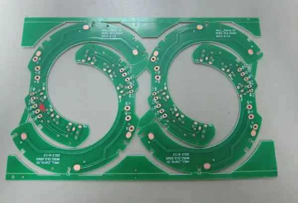
Considerations for Reliable Layout Element Placement in PCB Design
Printed circuit board technology will never stop. At present, the engineering team is studying ways to improve circuit density by using devices with finer spacing. When these components are placed on the PCB, the error amplitude will decrease with the pin spacing. Let's look at how to enable these parts on the assembly line.
The first step in mass production of PCB components is to prepare the circuit board to contain the components. Before starting the assembly process, the plates can be dehydrated in the oven. Even if they are packed in a sealed container containing a small bag of desiccant, water can still only enter into one sponge like dielectric material molecule at a time. Pre baking them will release steam that may affect reflow soldering.
Best choice: pure mixing of surface mount components
Ideally, in terms of pin spacing and other physical aspects, all parts on the board will use the same type of technology and will be roughly the same type of component. Higher and higher components and smaller and lighter components are not a good combination. Tall people create shadows in areas that are not so hot around them.
Most component data sheets contain some welding instructions. The recommended paste type may be specified within the particle size range. A graph showing the thermal curve may give the best results. First, preheat rises to near reflow temperature, then reaches the peak of welding temperature, and then cooling period. All heat curves covering the components on a particular board will show results that are similar but not exactly matched to the recommended process window.
Your assembly plant is very attractive to the output. For them, the perfect circuit board has all the components in the same direction. They will all be surface mounted and on the same side of the board. Avoid using components with hidden leads, or leave extra space as a "paddock" where the repair nozzle is in full contact with the board surface. If they do not need to disassemble and solder a stack of passive components, but some of them do want to be close to specific pins, the efficiency will be higher.
Precautions for using fine pitch components
If fine pitch equipment is used, it will also have a pair of local reference marks to allow the pickup head to record its exact position for more accurate placement. These benchmarks will be complementary to board level benchmarks and can be shared among devices if there is symmetry between them. Ideally, each component will face a basic direction with the same and uniform polarity markings.
The real world doesn't work that way, but that's a goal. In the 30 years of PCB layout, I have never made all capacitors and resistors in the same direction, let alone all polarization components. The idea is to let people know how to place components for optimal performance, and determine a general direction for using this angle as much as possible.
OK, so you can prepare the almost perfect layout and be ready to assemble the circuit board. The next step is to apply solder paste. Depositing solder paste on PCB must be accurate and repeatable. Smaller plates or plates with complex profiles will require subpanels to be assembled.
At the same time, larger boards often contain componentless areas at the edges for placement and soldering processes. Usually, we look for a 5mm wide componentless space on the longer edge of the board so that the machine can catch them. Mold holes will facilitate repeatable and error free orientation of fabs, templates, pick and place, and test fixtures. Three alignment holes provide this assurance.
In addition to the larger fab panel, you can also use the assembly subpanel to return to the board. Consider the orientation of the components before selecting the edges that require the rails to be mounted. The surface mounted and through hole assemblies have the best direction of travel through the welding table. The focus is on preventing solder bridges and other defects (we will discuss them later).
Passive components like to pass through the other end of the oven and enter the process flow. In this way, both pads can see the same temperature curve at the same time. If one side reflows and solidifies before the other side, defects such as cold solder and solder interference are more likely to occur. The appearance of cold solder is dull, and there will be no fillet indicating proper wetting. The disturbed solder has an irregular profile, indicating some movement of the component during the critical transition from liquid to solid solder. These are the two defect categories that lead to potential defects, and they are the most serious defects.
Improperly placed components can also be lifted from one of the pads like a suspension bridge, although we call it a tombstone. I have encountered the case where ceramic and wire wound components actually crack due to the stress of different heat distribution curves. These defects occur because one end of the capacitor/inductor is close to the edge of the board and the other end is located on the inside of the board. In a reflux furnace, the edges become hotter as the temperature rises and falls faster during plate time.
The key element of reliable placement is the space between components. We want the shortest RF path, so this will be the first consideration. A wide bus also requires close proximity between the driver and receiver. Almost all decoupling capacitors will benefit from being close to the relevant power supply pin. The crystals shall be kept in traction for a short time. It seems that every widget wants a point next to the main chip.
Even so, the more breathing space a component has, the longer the expected time until degradation and failure. Close together but not crowded? How to selectively separate according to the needs of coexistence and thermal management. There are too many factors pulling us in different directions. The smart arrangement made all participants equally nervous, and no one was too nervous.
Sharing your work along the way is more important than ever. Our main goal is to develop products that everyone can buy at the end of the design cycle. The last thing we want is to design the board as a giant ship that runs aground and gets stuck in the canal. This is the feeling when the various factions are still trying to resolve their differences.
Getting a complete placement is more difficult than getting a complete design. Usually, I submit the first presentation location when the receive and send chains are linked. All components are colored by their schematic pages. Even if the reference mark must be disturbed, make sure. At least some of them survived until they were released. The circuit board assembly and circuit board processing manufacturers explain the reliable layout components placement precautions of circuit board design.


Just upload Gerber files, BOM files and design files, and the KINGFORD team will provide a complete quotation within 24h.