
Professional PCB manufacturing and assembly
Building 6, Zone 3, Yuekang Road,Bao'an District, Shenzhen, China
+86-13410863085Mon.-Sat.08:00-20:00

The money saving PCB design skills can make your production efficient
There is a very simple equation for calculating profit. Fixed costs and overhead must be less than the revenue figure to have any profit. The first batch of equipment just went out owes the company all the non recurring engineering costs. The item will be displayed in red until the difference between the unit price and the unit price is fully repaid.
In many sectors of the economy, especially the commercial sector, the cost of goods sold (COGS) is almost equal to the selling price, which means that the profit after taking into account the indirect costs is very small. Please note that PCB design is part of the overhead. Before the financial situation of the project reaches the break even point, many units must leave the factory and find consumers. The product cycle is so fast that price erosion is squeezing profits from the beginning. There is no doubt that consumer hardware is a difficult game.
The competition among players has put us on the road of continuous improvement. Sitting down while others try to seize your market share is actually going backwards, so it is natural for us to think that we must continue to innovate our products. These new functions, no matter what they are, may be added to the bill of materials, thus increasing variable costs. We can use several ways to save money to mitigate this blow.
The first mover has more leeway. No one else can gain this premium pricing advantage. Someone will always reflect your company's blueprint, so lead is easy to decay, but it is definitely worth owning and retaining. Design victory can bring more design victory, but the premise is that we must implement the subsequent new product introduction. Victory creates enthusiasm.
I'm not thinking about losing, so I need to keep my energy in line with my attitude and will, so as to proceed as planned as possible. By monitoring progress against expectations, you can know if the product schedule has started to slide. Early action is the best way to address this ongoing concern.
One thing you might know at first is the expected end date. From now on, milestones should be established to complete library, schematic diagram, layout, key wiring, simulation and other work. Each milestone should end with a meeting at which we can check all the items needed to continue the task. Next door.
For the sake of authenticity, suppose the schematic completion date is here, but the schematic is not. A meeting must be held at any rate. Take this as the central point, and figure out how to meet your colleagues by completing a large number of high-quality circuit board layout work in a short time.
If your personal efforts are not enough, some of these things can be completed simultaneously with other design resources. If you know you need help determining the deadline, it's up to you. The fees of the service bureau seem very high, which may exceed your own fees.
If everything goes according to plan, it will pay off. Most of the revenue comes before the imitators release their versions. The first person to use a similar product may leave it temporarily, or even replace the first mover. That's not normal. Become a primitive, and retain the primitive by developing something better than the previous iteration. Spend money to make money or lag behind the market share of medium-sized products.
Data sheets will be provided shortly after the order is placed. Some library generators also execute schematic symbols and include step models of parts.
You know that PCB can't be better than the package of basic components. A wise designer will carefully check the new geometry before using it. If the management is correct, you can quit making footprints, just check them, and then add them to your library.
Strengthen the circulation between product designer data and PCB data
We obtain mechanical data in different ways. In general, there are several layers of shapes that define alignment and component reservation/reservation areas. Sometimes, well, in most cases, the mechanical engineer will have some small faults in the data provided for the first test. What I have seen and accepted over the years may make this a long story.
So, this is an example. When the clearance height under the shielding layer needs to be enough to accommodate the parts but the parts are marked too high, set it to zero. It is incorrect to mark all parts too high, however, I can use it. One approach is to ignore design rule checking. The other is to edit the properties to enforce the actual clearance.
Both approaches have risks. By pointing out the burrs that have occurred, you can reach a better position, and the mechanical data can be correctly determined by design. Experience has shown that there are few mechanical outlines at first. Some properties may be pending.
After these items are eliminated, please continue to feed back your modifications to their basic dimensions. The purpose of this is to reduce the trouble of capturing slightly different contours on the road. Time is money, so try to streamline these occasions. The earlier you are processed, the less impact it will have. As planned, this is closely related to the cleaning schematic. In the early days of the game.
When your goal is to clean up the process, you will not become a pest. The requested framework is designed to have good design integrity, rather than following the details of ECAD tools. Except for the switching gate, we usually do not change the netlist. For the same reason, we should not formulate routines for the purpose of "fixing" MCAD data. Every change can be improved, but it would be better if there were no self defeats. The conversation with the team paid off.
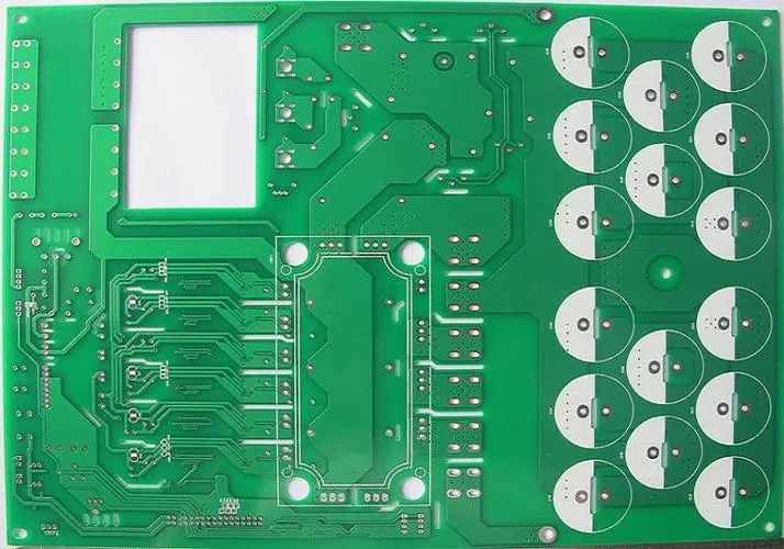
Use the side of the board
say it again! Use one side of the circuit board for components. This is probably the greatest help you can give the assembly plant. If the shape allows filling on one side of the PCBA, you will be ahead of the game by placing the part on the second and second sides. Most MCU will be able to work in this arrangement. Explore feasibility.
The single panel can pass through the reflux furnace. In order to weld both sides of a PCB board, one side must be filled only on a small part of it. The first pass on the double-sided plate will use a higher temperature solder so that reflow will not occur again when welding the other side. Even so, the heavier components on the secondary (down) side may need glue to ensure that they do not loosen.
Limit BOM to one technology. Similarly, we are considering reducing processes. SMT is a popular technology, so it is the best choice to provide end-to-end solutions for your part selection. Mixing surface mount and through-hole parts is a cost driver. Wave soldering, including surface mounting, is more difficult. Like oil and water, SMT and through-hole are poorly mixed.
Avoid or minimize high-density interconnects
This can also be tricky. It is difficult to fill in the bill of materials without some ball grid array (BGA) packages (pin spacing requires the use of micro through-hole). These tiny vias are formed by lasers, and a wafer factory must create them layer by layer. The result is that each layer of micro through-hole needs to go through a laminating press.
It's a waste of time, which means it costs a lot of money. The press is an expensive large machine, which consumes a lot of power. This may be a bottleneck in the process of small manufacturers. No matter how big they are, they need to be laminated sequentially because it requires more work.
To solve all these problems, you will need to purchase chips that use quad flatpacks or other packages with only peripheral pins. Finding a second source would be another tedious task. With regard to the assembly line, they still had to perform an X-ray inspection of the board to find the gap in the solder joint of the thermal pad in the middle of most of these packages. We often use the board system. One of the differences between boards is the required technology. Maximizing the use of the cheapest board may help reduce the size of the system's main PCB.
If execution is not a problem, creativity and innovation will be rewarded. When iterating over the list of upgrades required, it is usually best to bring a set of functions to the site and study the benefits and costs. The so-called agile development can help you guide the product from concept to concrete through planned steps. Functional creep is the key, but it is necessary to closely meet the market demand, so that you can have products that win short-term competition, and develop into cost competitive models according to market requirements. Circuit board assembly and circuit board processing manufacturers explain money saving PCB design skills to make your production efficient.


Just upload Gerber files, BOM files and design files, and the KINGFORD team will provide a complete quotation within 24h.