
Professional PCB manufacturing and assembly
Building 6, Zone 3, Yuekang Road,Bao'an District, Shenzhen, China
+86-13410863085Mon.-Sat.08:00-20:00

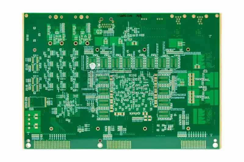
Design performance requirements for multi substrate PCB
The design performance of a multi substrate PCB is similar to that of a single substrate or a dual substrate. That is, it is important to avoid filling too many circuits with too little space, which may result in unrealistic tolerances, high inner layer capacity, or even endanger the safety of product quality. Therefore, the performance specification should consider the complete evaluation of thermal shock, insulation resistance, welding resistance, etc. of the inner layer circuit. The following describes the important factors that should be considered in the design of multi substrate PCB.
1、 Mechanical design factors
Mechanical design includes the selection of appropriate plate size, plate thickness, plate lamination, inner copper cylinder, aspect ratio, etc.
1 Plate size
The board size shall be optimized according to application requirements, system box size, limitations of circuit board manufacturers and manufacturing capabilities. Large circuit boards have many advantages, such as fewer substrates and shorter circuit paths between many components, which can achieve higher operation speed. Besides, each board can have more input and output connections. Therefore, large circuit boards should be preferred in many applications. For example, in personal computers, large motherboards are seen. However, it is difficult to design the signal line layout on the large board, which requires more signal layers or internal wiring or space, and the heat treatment is also difficult. Therefore, the designer must consider various factors, such as the size of the standard board, the size of the manufacturing equipment and the limitations of the manufacturing process. 1PC-D-322 gives some guidelines for selecting standard printed circuit/board sizes.
2 Plate thickness
The thickness of a multi substrate PCB is determined by many factors, such as the number of signal layers, the number and thickness of power boards, the aspect ratio of aperture and thickness required for high-quality drilling and electroplating, the length of component pins required for automatic insertion, and the type of connection used. The thickness of the entire circuit board consists of the conductive layer, copper layer, substrate thickness and prepreg thickness on both sides of the board. It is difficult to obtain strict tolerance on the composite multi substrate PCB, and about 10% of the tolerance standard is considered reasonable.
3 Lamination of plates
In order to reduce the probability of board twisting to a minimum and get a flat finished board, the layering of multi substrate PCBs should be symmetrical. Namely, it has an even number of copper layers and ensures that the thickness of copper is symmetrical with the copper foil pattern density of the sheet layer. Generally, the radial direction of the construction material used for lamination (e.g. glass fiber cloth) should be parallel to the edge of the laminate. Because the laminated plate shrinks along the radial direction after bonding, the layout of the circuit board will be distorted, showing variable and low spatial stability.
However, by improving the design, the warpage and distortion of the multi substrate PCB can be minimized. Through the average distribution of copper foil on the whole layer and ensuring the structural symmetry of multi substrate PCB, that is, ensuring the same distribution and thickness of prepreg materials, the purpose of reducing warpage and distortion can be achieved. The copper and rolled layer shall be made from the center layer of the multi substrate PCB to the outermost two layers. The specified minimum distance (dielectric thickness) between two copper layers is 0.080mm.
It is known from experience that the minimum distance between two copper layers, that is, the minimum thickness of the prepreg after bonding must be at least twice the thickness of the embedded copper layer. In other words, if the thickness of each layer of two adjacent copper layers is 30 μ m. The thickness of prepreg shall be at least 2 (2 x 30 μ m) =120 μ m. This can be achieved by using two layers of prepreg (the typical value of fiberglass fabric is 1080).
4 Inner copper foil
The most commonly used copper foil is 1oz (1oz per square foot of surface area). However, for dense boards, the thickness is extremely important, and strict impedance control is required. Such boards need to be used
0.50z copper foil. For the power supply layer and ground plane, it is better to choose copper foil of 2oz or heavier. However, heavy etching of copper foil will reduce controllability, and it is not easy to achieve the desired line width and spacing tolerance pattern. Therefore, special processing techniques are required.
5 holes
According to the pin diameter or diagonal size of components, the diameter of plated through-hole is usually kept between 0.028 0.010 in, which can ensure sufficient volume for better welding.
6 Aspect ratio
The "aspect ratio" is the ratio of the thickness of the plate to the diameter of the borehole. It is generally believed that 3:1 is the standard aspect ratio, although a height aspect ratio like 5:1 is also commonly used. The aspect ratio can be determined by factors such as drilling, removing glue residue, or back etching and electroplating. When the aspect ratio is maintained within the production range, the vias should be as small as possible.
2、 Electrical design factors
Multi substrate PCB is a high-performance and high-speed system. For higher frequencies, the rise time of the signal decreases, so the control of signal reflection and line length becomes critical. In the multi substrate PCB system, the requirements for the controllable impedance performance of electronic components are very strict, and the design should meet the above requirements. The factors that determine the impedance are the dielectric constant of the substrate and the prepreg, the wire spacing on the same layer, the thickness of the interlayer medium and the thickness of the copper conductor. In high-speed applications, the laminating sequence of conductors in multi substrate PCBs and the connection sequence of signal nets are also crucial. Dielectric constant: The dielectric constant of the substrate material is an important factor in determining the impedance, propagation delay and capacitance. The dielectric constant of the substrate and prepreg using epoxy glass can be controlled by changing the percentage of resin content.
The dielectric constant of epoxy resin is 3.45 and that of glass is 6.2. By controlling the percentage of these materials, the dielectric constant of epoxy glass may reach 4.2 - 5.3. The thickness of the substrate is a good illustration for determining and controlling the dielectric constant.
Prepreg with relatively low dielectric constant are suitable for RF and microwave circuits. In RF and microwave frequencies, the signal delay caused by lower dielectric constant is lower. In the substrate, a low loss factor minimizes electrical losses.
The prepreg material ROR 4403 is a new material produced by ROGERS. This material is compatible with other substrates (such as RO 4003 or RO 4350 for microwave boards) used in standard multi substrate PCB (FR - 4 material) structures. The circuit board assembly and circuit board processing manufacturers explain the important factors that should be considered in the multi board PCB design.


Just upload Gerber files, BOM files and design files, and the KINGFORD team will provide a complete quotation within 24h.