
Professional PCB manufacturing and assembly
Building 6, Zone 3, Yuekang Road,Bao'an District, Shenzhen, China
+86-13410863085Mon.-Sat.08:00-20:00

Among the commonly used types of printed circuit boards, the matters needing attention in layout design are detailed as follows: 1) Single panel: this type of panel is usually used when the cost requirement is low. In layout design, components or jumpers are sometimes needed to skip the power supply
Among the commonly used types of printed circuit boards, matters needing attention in PCB design are detailed as follows:
1) Single panel: This type of panel is usually used when the cost requirement is low. In layout design, components or jumper wires are sometimes required to skip the routing of circuit boards. If the number is too large, you should consider using double-sided boards.
2) Double sided board: PTH can be used or not. Because PTH boards are expensive, they can only be used when the complexity and density of the circuit require.
In general, the choice of single sided PCB or double-sided PCB must meet the most effective cost utilization. According to experience, the cost of double-sided printed boards with plated through holes is 5-10 times as much as that of single panels. Similarly, the cost of assembling components is also an important aspect to be considered. The cost of assembling components (manually) of a single-sided printed circuit board is about 25% - 50% of the cost of the circuit board, while the cost of assembling components of a double-sided printed circuit board with PTH is 15% - 30% of the cost.
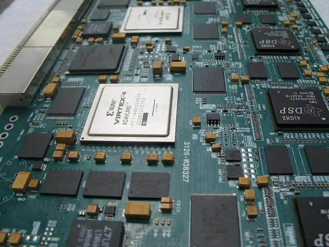
The printed circuit board not only provides mechanical support, but also plays a role in connecting the components installed on it. Therefore, for the designers of printed circuit boards, it is necessary to know the overall physical size (frame size) of the panel, the location of mounting holes, height restrictions and relevant details.
Main factors to be considered in mechanical design of printed circuit board
1) The best panel size suitable for PCB fabrication;
2) Position of panel mounting hole, bracket, plywood, clip, shielding box and radiator;
3) Suitable fixing device for heavy components;
4) Suitable hole diameter for component installation;
5) The assembled circuit board shall have compression resistance and seismic resistance during transportation;
6) Assembly mode of circuit board (vertical installation/horizontal installation);
7) Cooling mode;
8) Special placement requirements for components are similar to those operated on the front panel, such as buttons, rheostats, etc.
Steps of PCB layout design
Before the layout design, a complete and detailed description of the circuit is required, mainly including the following aspects:
1) Schematic diagram, including details of components, connections and specifications of edge connectors.
2) List of components, including name, specification, model and PCB manufacturer of components.
3) Mechanical specifications, including the size and shape of the board, mounting holes, marking of the height restricted area of PCB components, position of edge connectors, etc.
4) Printed circuit board specification, single panel, double sided board or multi substrate, with or without plated through-hole.
5) Drawing specifications, including the type and size of pads, the width and spacing of wires.
6) Electrical specifications, such as the placement of components and parts shall be limited by the heat generated, capacitance or inductance contribution, grounding, critical length of wiring, etc.
7) PCB data operation.


Just upload Gerber files, BOM files and design files, and the KINGFORD team will provide a complete quotation within 24h.