
Professional PCB manufacturing and assembly
Building 6, Zone 3, Yuekang Road,Bao'an District, Shenzhen, China
+86-13410863085Mon.-Sat.08:00-20:00

Circuit board manufacturers share how to learn circuit board design from scratch
The circuit board assembly and circuit board processing manufacturers explained that they had not learned PCB Layout and learned PCB design knowledge from scratch.
I haven't learned PCB Layout, so you can start from scratch with me. A simple question, where do I start? The question is simple, but the answer is complex.
First of all, you should learn some basic knowledge about the commonly used software: Allegro, Pads, Protel, Orcad, etc. (please refer to the relevant materials for the introduction of each software).
Before starting PCB Layout, you should have a good understanding of PCB.
PCB board, specification, current process level.
PCB device information, such as packaging and related dimensions.
Placement and connection of PCB devices, such as how to place some special devices.
PCB wiring rules and identification.
These are about which devices to use, how to wire them, and on which motherboards to place them.
Details are as follows:
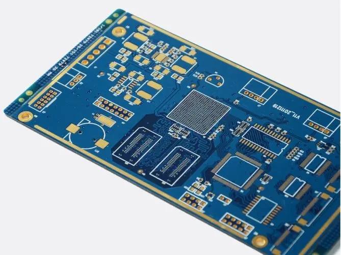
1、 PCB board
Common base plates include: FR-4 (epoxy resin/glass fiber), aluminum base plate, ceramic base plate, paper core plate, high TG (glass material jump temperature) value plate, high-frequency plate, mixed multilayer plate, etc. Generally, the factory will give the maximum and minimum sizes that can be produced, such as the maximum size of 600X1000mm, the minimum size of 2X10mm, etc. If it is a multilayer board, there will be a limit on the number of layers of the board and the thickness of the board (the thickness is usually 0.5-6mm). Other substrates have various shapes, such as common motherboards, video cards, mobile phone boards, etc. There are also changes in the design of flexible materials such as flat wires. The selection of these materials is related to the product and cost.
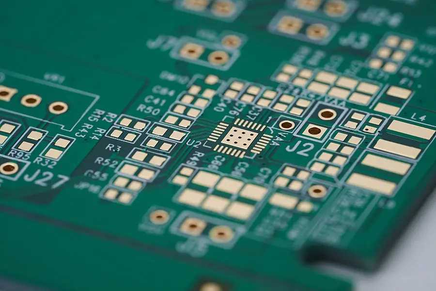
2、 Device information
Draw the schematic diagram from orcad, and then turn out Allegro netlist. Double click the device in the orcad capture to see that the pcb footprints are assumed to be SO16 in the attribute, and HEF4051B in the source package. It is SO16 in netlist! HEF4051B: U01, generate device files from the principle from the capture Allegro netlist command. For example, SO16.txt will describe the device, pin pin and related information. SO16 refers to package form, while HEF4051B is a real device.
Common packaging forms: DIP dual in line package, QFP square flat package, SOP small frame package, PLL lead chip carrier, BGA ball grid array package, etc. For details, please refer to relevant materials. Design pads and connection holes according to the data you get. Cadence PSD is designed with pad designer.
There are five types of pads:
1, regular: A solid positive pad (black), which can be round, square, or elliptical.
2. Thermal: relief flower shaped figure, replacing regular pad for better heat dissipation.
3. Anti pad: negative pad (clear), which is usually cut from the square to round, to prevent pins from connecting to other metal layers.
4. Shapes: User defined graphics
5. Flash: User defined aperture
Via is called through hole. If it passes through the whole plate layer, it is through via. If it only appears on one surface, it is blind via. If it appears on the interior (not visible on both surfaces), it is built via.
Pads and through holes set by pad designer will be used when creating symbols. Start Allegro ->new ->package symbol (wizard), and input the size, type and previously set pad of the corresponding device. (Note: the first pin should be identified), and then the symbols corresponding to the device will be generated. The names of these symbols should be consistent with the names of pcb footprints, so that no error occurs when assigning names. (Save as. dra file)
Start Allegro ->new ->board to generate a motherboard file, draw the shape of the board with lines, assign the keepin router/package as the placement and routing area, and save it as Brd file. Then import logic reads the Allegro netlist output from orcad. (If illegal characters appear in single quotation marks, parentheses are comments).
After the input is successful, you can place the device manually, and use logic ->logic assign refdes to select and name the device. If it is correct, flying lines will appear. After the placement is successful, you can refer to the routing strategy written by experts to conduct routing and simulation.
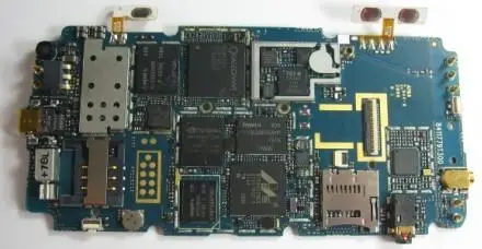
3、 Placement and connection of devices
There are also many considerations for placement of devices, such as the direction of the board, device functions and related interference, placement of special devices, heat dissipation of devices, and ease of wiring. The circuit board assembly and circuit board processing manufacturers explained that they had not learned PCB Layout and learned PCB design knowledge from scratch.


Just upload Gerber files, BOM files and design files, and the KINGFORD team will provide a complete quotation within 24h.