
Professional PCB manufacturing and assembly
Building 6, Zone 3, Yuekang Road,Bao'an District, Shenzhen, China
+86-13410863085Mon.-Sat.08:00-20:00

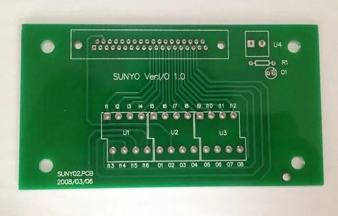
Considerations for PCB layout and precautions for SD card PCB design
In PCB design, layout is a very important link. The quality of the system layout will directly affect the wiring effect. A reasonable layout can have the following advantages:
·The reliability of the system is improved.
·Make the volume of the system smaller;
·Save the space of the circuit board to reduce the cost;
Generally speaking, there are two ways of PCB layout, one is interactive PCB layout, the other is automatic PCB layout. In practical applications, the interactive layout can be used on the basis of automatic layout for adjustment, and the gate circuit can also be redistributed according to the routing during layout. For example, two gate circuits can be exchanged to make it the best layout for easy wiring.
Whether a product is successful or not, first, we should pay attention to the internal quality, and second, we should give consideration to the overall beauty. Only when both are perfect can we consider the product successful. Considering the overall beauty of PCB layout, the layout of components on a PCB should be balanced and orderly.
Another important problem of PCB layout is the size of PCB. The size of PCB should be consistent with the production of processing drawings, meet the requirements of PCB manufacturing process and have positioning marks.
It is also necessary to consider whether the components of PCB have conflicts in two-dimensional and three-dimensional space. For example, the thermal sensor should be far away from the heat source.
Some high-power components in the PCB layout also need to add heat sink, and the size of the heat sink should also be considered.
SD Card PCB Design Considerations
1. Pay attention to the accuracy of the material number and plate name. The material number and plate name include the name of the schematic diagram, the schmetic file name under the schematic diagram, and the document description part in the lower right corner of the schematic diagram. Pin without network connection in schematic diagram shall be crossed. If there is a network lead connector before, there is a network name after deleting the network name, such as NET-XXX, which is a system number. At this time, DRC will make an error, and the leader needs to be completely deleted and crossed.
2. Export CAD files to the manager of the engineering department with the suffix DXF. Note that the unit is mm.
3. For SD card layout board, first place the documents according to the actual needs. Coordinate positioning shall be adopted for placing files to ensure the accuracy. Note that the master controller and FLASH should not be close to the edge, and at least 0.5mm space should be reserved for production.
4. For wiring, the primary and secondary relationship between each signal line must be clarified first. The main signal lines are CLK and VSD. Generally speaking, CLK signal lines need to be surrounded by ground wires or land.
5. The ground signal shall be paved with copper after all wiring is completed and observed to make the land as large as possible and the gap between signal lines as small as possible, so that the land can be expanded. The ground of the top layer and the bottom layer shall be reliably connected. In the case of copper sheets on the upper and lower layers, holes shall be punched for connection.
6. For test points, try to distribute them in a balanced state, and the spacing should be consistent, so that they can be fixed properly.
7. To make boards, the files to be exported include GERBER files and panel drawings. Pay attention to the material requirements that need to be noted when requesting the opening of boards. PCB assembly and PCB processing manufacturers explain the aspects that should be considered in PCB layout and SD card PCB design considerations.


Just upload Gerber files, BOM files and design files, and the KINGFORD team will provide a complete quotation within 24h.