
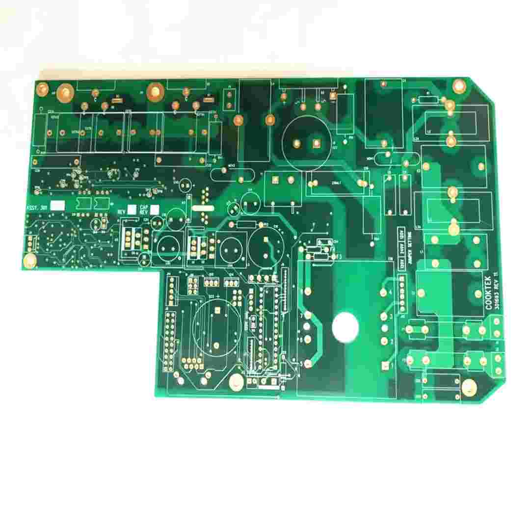
Professional PCB manufacturing and assembly
Building 6, Zone 3, Yuekang Road,Bao'an District, Shenzhen, China
+86-13410863085Mon.-Sat.08:00-20:00

Differences and Usage of Polygon Pour, Fill and Plane in Altium, Circuit Board Design
The circuit board manufacturer explains the difference and usage of Polygon Pour, Fill and Plane in Altium
Polygon Pour: Copper pouring. Its function is similar to that of Fill, which is also to draw large areas of copper skin; However, the difference lies in the word "pouring". Copper pouring has a unique intelligence, which can actively distinguish the vias and solder joint networks in the copper pouring area. If vias and solder joints belong to the same network, copper pouring will connect vias, solder joints and copper sheets according to the set rules. On the contrary, a safe distance will be kept between the copper sheet and the vias and solder joints. The intelligence of copper filling is also reflected in its ability to automatically delete dead copper.
Polygon Pour Cutout: establish a copper digging area in the copper pouring area. For example, some important networks or components need to be hollowed out at the bottom, such as common RF signals. There is also RJ45 area under the transformer.
Polygon Pour: Cut the copper pouring area. For example, if you need to optimize or reduce the copper pouring area, you can use Line to divide the reduced area into two copper pouring areas, and delete the unwanted copper pouring areas directly.
Fill means to draw a solid copper sheet to connect all wires and vias in the area together, regardless of whether they belong to the same network. If there are two networks VCC and GND in the drawn area, use the Fill command to connect the elements of these two networks together, which may cause a short circuit.
To sum up, Fill will cause short circuit, so why use it?
Although Fill has its shortcomings, it also has its use environment. For example, when there are LM7805, AMC2576 and other high current power supply chips, a large area of copper sheet is required to cool the chip, so there can only be one network on the copper sheet, and it is just right to use the Fill command.
Therefore, the Fill command is often used in the early days of circuit board design. After the layout is completed, use Fill to draw all the special areas to avoid making mistakes in the subsequent design.
In short, these two tools are used together in the process of circuit board design.
Plane: plane layer (negative film), applicable to the whole board with only one power supply or ground network. If there are multiple power supply or ground networks, you can use line to draw a closed box in a power supply or region, and then double click the closed box to assign a corresponding power supply or ground network to this region. It can reduce a lot of engineering data compared with add layer, and the computer response speed on high-speed PCB is faster. You can deeply experience the benefits of plane in the process of revision or modification.
Method 1: When repairing copper, use PLANE [shortcut key P+Y] to repair obtuse angle.
Method 2: Select the copper sheet to be trimmed, and press the shortcut key M+G to adjust the shape of the copper sheet at will. Circuit board assembly, circuit board design, and circuit board processing manufacturers explain the differences and uses of Polygon Pour, Fill, and Plane in Altium.


Just upload Gerber files, BOM files and design files, and the KINGFORD team will provide a complete quotation within 24h.