
Professional PCB manufacturing and assembly
Building 6, Zone 3, Yuekang Road,Bao'an District, Shenzhen, China
+86-13410863085Mon.-Sat.08:00-20:00

The complexity level and application scope of PCB (printed circuit board) have been rapidly developed. Those who are engaged in high frequency must have corresponding fundamental theoretical knowledge and rich experience in manufacturing high frequency PCB. That is to say, both the drawing of PCB schematic diagram and PCB design should be considered from the high frequency working environment where they are located to design an ideal PCB.
1 Planning design
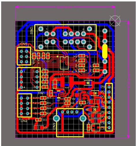
Although it has the function of automatic planning, it can not fully meet the working requirements of high-frequency circuits. It is often necessary to rely on the experience of PCB designers, and according to the detailed situation, first use manual planning to optimize and adjust the position of local components, and then separate automatic planning to complete the overall design of PCB. Whether the planning is reasonable or not directly affects the product life, stability, EMC (electromagnetic compatibility), etc. It is necessary to comprehensively consider the overall planning of the circuit board, the connectivity of wiring, the manufacturability, mechanical structure, heat dissipation, EMI (electromagnetic interference), reliability, signal integrity, etc.
Generally, first place the components at fixed positions related to mechanical dimensions, then place special and large components, and finally place small components. At the same time, it is necessary to coordinate the requirements of wiring. The placement of high-frequency components should be as compact as possible, and the wiring ability of signal lines should be as short as possible, so as to reduce the interference of signal lines.
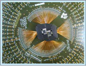
High frequency circuits are often highly integrated and wiring density is high. Multilayer boards are necessary for wiring and an effective way to reduce interference. Protel for Windows V1.5 can provide 16 copper wire layers and 4 power supply layers. Reasonable selection of layers can greatly reduce the size of printed boards, make full use of intermediate layers to set shielding, better complete the nearby grounding, effectively reduce parasitic inductance, effectively shorten the transmission length of signals, and greatly reduce the interpenetration interference between signals. All these are beneficial to the reliable work of high-frequency circuits. When the same kind of data is displayed with materials, the noise of the four layer board is 20dB lower than that of the double-sided board. However, the higher the number of layers, the more complex the manufacturing process, and the higher the cost. Fast proofing of TG PCB
PCB design
The lead between pins of high-speed circuit devices shall be bent as little as possible. The lead wire of high frequency circuit wiring should preferably be full straight line, and 45 degree broken line or circular arc rotation can be used for the required rotation. This request is only used to improve the fixation strength of the steel foil in the low-frequency circuit, while meeting this request in the high-frequency circuit can reduce the external transmission and mutual coupling of high-frequency signals. The following two settings can be made in advance when using Protel wiring: first, the 45/90 Line or 90 ArcLine wiring can be scheduled in the Track Mode submenu of the Options menu; Second, when Add Arcs is selected in the RoutingPasses dialog box opened by the Setup Autorouter item in the Auto menu, the corner will be arced when the automatic routing is completed.
Burial/process flow and technology
The next lamination method is generally adopted. Namely:
Cutting --- core board (equivalent to conventional double-sided board or multilayer board) --- lamination --- the following process is the same as that of conventional multilayer board.
(Note 1): The core plate refers to the embedded/blind hole multilayer plate formed according to the structural requirements after the double-sided plate or multilayer plate formed by conventional methods. If the thickness diameter ratio of holes in the PCB core board is large, the hole plugging treatment should be stopped to ensure its reliability. Fast proofing of TG PCB
Nowadays, the motherboard and graphics card both use multilayer boards, which greatly increases the area that can be wired. More single or double sided wiring boards are used for multilayer boards, and a layer of insulating layer is placed between each layer of boards and then pressed together. The number of layers of a PCB board represents that there are several independent PCB wiring layers. Usually, the number of layers is even, and includes the two outermost layers (no computer sound). Common PCB boards are generally 4-8 layers. The number of layers of many PCB boards can be seen from the section of PCB boards. But in practice, no one can have such good insight. So, let's teach you another way.
The circuit connection of multilayer boards is through the technology of embedded hole and blind hole. The main board and display card mostly use 4-layer PCB boards, while some use 6-layer, 8-layer or even 10 layer PCB boards. If you want to see how many layers a PCB has, you can identify it by looking at the guide hole. Since the 4-layer boards used on the main board and the display card are the 1st and 4th layers of wiring, the other layers have other uses (ground wire and power supply). Therefore, like the double-layer board, the pilot hole will pierce the PCB board. If some pilot holes appear on the front of the PCB, but cannot be found on the back, it must be 6/8 layers. If the same pilot holes can be found on the front and back of the PCB, it is naturally a 4-layer board. High fine TG PCB


Just upload Gerber files, BOM files and design files, and the KINGFORD team will provide a complete quotation within 24h.