
Professional PCB manufacturing and assembly
Building 6, Zone 3, Yuekang Road,Bao'an District, Shenzhen, China
+86-13410863085Mon.-Sat.08:00-20:00


Etching Technology and Process Control of Printed Circuit Board
Process printed circuit board (PCB) is a complex physical and chemical reaction process from optical board to display circuit graphics At present, the typical process of PCB processing is adopts "graphic electroplating method" That is, the copper foil is pre coated with a layer of lead tin anti-corrosive coating, which is retained on the outer layer of the copper foil printed circuit board. That is, the graphic part of the circuit, and then the remaining copper foil is chemically etched, which is called etching
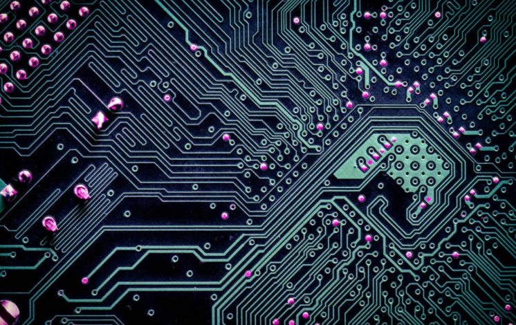
Etching type of circuit board

It should be noted that during the etching process, there are two layers of copper on the printed circuit board. In the outer layer etching process, only one layer of copper must be completely etched, and the rest will form the final required circuit. The characteristic of this pattern electroplating is that the copper plating layer only exists below the lead tin resistance layer.
Another process is that the entire printed circuit board is plated with copper, and the part except the photosensitive film is only a tin or lead tin corrosion resistant layer. This process is called "full plate copper plating process". Compared with pattern electroplating, the biggest disadvantage of full plate copper plating is that copper must be plated twice anywhere on the plate surface and must be corroded during etching. In this case, when the wire width is very thin, a series of problems will occur. At the same time, the side corrosion will seriously affect the uniformity of the line.
In the processing technology of external circuit of printed circuit board, another method is to replace metal coating with photosensitive film as anti-corrosion coating. This method is very similar to the inner layer etching process. You can refer to the etching in the inner layer manufacturing process.
At present, tin or lead tin is the most commonly used resist layer, which is used as an etchant in the ammonia etching process. Ammonia etchant is a widely used chemical solution, which has no chemical reaction with tin or lead tin. Ammonia etchant mainly refers to ammonia/ammonia chloride etchant.
In addition, ammonia/ammonia sulfate etching solutions can also be purchased on the market. Copper in sulfate etching solution can be separated by electrolysis after use, and can be reused. Due to its low corrosion rate, it is rarely seen in actual production, but it is expected to be used for chlorine free etching.
Someone tried to use sulfuric acid hydrogen peroxide as an etchant to etch the external pattern. Due to many reasons such as economy and waste liquid treatment, this process has not been widely used in commercial sense. In addition, sulfuric acid hydrogen peroxide cannot be used to etch the lead tin corrosion resistant layer, and this process is not the main method of PCB outer layer production. In this regard, most people pay little attention to it.
PCB Etching
Etching quality and existing problems of printed circuit board
The basic requirement for etching quality is to completely remove all copper layers under the resist layer, and that's all. Strictly speaking, if accurate definition is required, the etching quality must include the consistency of conductor line width and the degree of side corrosion. Due to the inherent characteristics of the current corrosion solution, it can not only corrode downward, but also corrode left and right. This lateral corrosion is almost inevitable.
Side etching is often discussed in etching parameters. It is defined as the ratio of side etching width to etching depth, which is called etching factor. In the printed circuit industry, it varies greatly from 1:1 to 1:5. Obviously, a small side etch scale or a low etch factor is most satisfactory.
The structure of the etching equipment and etching solutions with different components can affect the etching factor or the side etching degree, or they can be controlled. Some additives can reduce the degree of side corrosion. The chemical composition of these additives is usually a trade secret, and their developers will not disclose it to the outside world.
In many ways, the etching quality existed long before the printed circuit board entered the etching machine. Due to the very close internal relationship between various processes or printed circuit processing processes, there is no process that is not affected by other processes and does not affect other processes. In the previous film removal process, even in more processes, there were many problems that were determined as etching quality.
For the etching process of external graphics, because its "countercurrent" image is more prominent than most PCB processes, many problems are finally reflected in it. At the same time, this is also because etching is the last step in a series of processes starting from film pasting and photosensitivity. After that, the exterior pattern was successfully transferred. The more connections you have, the more likely you are to have problems. This can be regarded as a very special aspect of the production process of printed circuits.
Theoretically, after the PCB enters the etching stage, in the process of graphic electroplating and processing the printed circuit, the ideal state should be: the total thickness of copper and tin or copper and lead tin after electroplating should not exceed the thickness of the electroplating sensitive film. Therefore, the electroplating pattern is completely blocked and embedded by the "walls" on both sides of the film. However, in actual production, the electroplating pattern of printed circuit boards around the world is much thicker than the photosensitive pattern after electroplating. In the process of electroplating copper and lead tin, there is a trend of horizontal accumulation because the coating height exceeds the photographic film, so there is a problem. The tin or lead tin resist layer covered above the line extends to both sides to form an "edge", covering a small part of the photoresist film below the "edge".
The "edge" formed by tin or lead tin makes it impossible to completely remove the film when removing it, leaving a small part of "residual glue" under the "edge". The "residual glue" or "residual film" left under the "edge" of the resist will lead to incomplete etching. The etched circuit forms a "copper root" on both sides, thus reducing the line spacing, resulting in the printed circuit board not meeting the requirements of Party A, and may even be rejected. Because of the rejection, the production cost of PCB circuit will increase greatly.
In addition, in many cases, dissolution is formed by reaction. In the printed circuit board industry, the residual film and copper may also accumulate in the corrosion solution and plug in the nozzles of corrosion machines and acid resistant pumps, which must be shut down for treatment and cleaning, thus affecting the work efficiency.
Equipment adjustment and interaction with corrosion solution
Ammonia etching is a fine and complex chemical reaction process in PCB processing. On the contrary, it is an easy job. Once the process is adjusted, continuous production can be carried out. The key is that once the machine is started, it needs to keep working continuously and should not be stopped. The etching process depends to a large extent on the good working conditions of the equipment. At present, no matter what kind of etching solution is used, high-pressure spraying must be used. In order to obtain neat lines and high-quality etching effect, nozzle structure and spraying pipeline must be strictly selected.
In order to obtain good side effects, many different theories have emerged, forming different design methods and equipment structures. These theories are often very different. However, all etching theories recognize the most basic principle, even if the metal surface comes into contact with fresh etching solution as soon as possible. The chemical mechanism analysis of the etching process also confirmed the above viewpoint. In ammonia etching, assuming that all other parameters remain unchanged, the etching rate is mainly determined by ammonia (NH3) in the etching solution. Recall that the interaction between the new solution and the etched surface has two main purposes: one is to flush out the newly generated copper ions; The second is to continuously provide ammonia (NH3) required for reaction.
In the traditional knowledge of the printed circuit industry, especially the suppliers of printed circuit raw materials, people realize that the lower the content of monovalent copper ions in ammonia etching solution, the faster the reaction speed, which has been confirmed by experience. In fact, many ammonia etchant products contain special coordination groups (some complex solvents) of monovalent copper ions, which are used to reduce monovalent copper ions (these are scientific secrets of their products with high reactivity). It can be seen that the influence of unit price copper ion is not small. If the unit price of copper is reduced from 5000 ppm to 50 ppm, the etching rate will be more than doubled.
Since a large number of monovalent copper ions are generated in the etching reaction process, and the monovalent copper ions are always closely combined with the complex groups of ammonia, it is difficult to keep their content close to zero. Through the action of oxygen in the atmosphere, the univalent copper can be converted into bivalent copper, and the univalent copper can be removed. This can be achieved by spraying.
This is the functional reason for allowing air to enter the etch box. However, if there is too much air, it will accelerate the loss of ammonia in the solution and reduce the pH value, which will still reduce the etching rate. Ammonia in solution also needs to be controlled. Some users use the method of passing pure ammonia into the etching tank. To this end, a pH meter control system must be added. When the pH value measured automatically is lower than the given value, the solution will be added automatically.
In the field of chemical etching (also known as photochemical etching or PCH), research work has begun and reached the stage of etching machine structure design. In this method, the solution used is divalent copper instead of ammonia copper etching. It is likely to be used in the printed circuit industry. In the PCH industry, the typical thickness of etched copper foil is 5 to 10 mils, which is quite large in some cases. Its requirements for etching parameters are generally stricter than those of PCB industry.
Circuit board etching
On the surface of the upper and lower plates, the etching states of the leading edge and the trailing edge are different
A large number of problems related to the etching quality focus on the etching part of the upper plate surface. It is important to understand this. These problems stem from the influence of the colloid structure produced by the etchant on the upper surface of the printed circuit board. Colloidal deposits on the copper surface, on the one hand, affect the jet force, on the other hand, hinder the supplement of fresh etching solution, resulting in a reduction in etching speed. Due to the formation and accumulation of colloidal structure, the upper and lower patterns of printed circuit boards are etched to different degrees. This also makes the first part of the printed circuit board in the etching machine easy to be completely etched or easy to cause excessive corrosion, because no accumulation was formed at that time and the etching speed was fast. On the contrary, when the parts entering the back of the printed circuit board enter, they have formed accumulation, and their etching speed is slowed down.
Maintenance of etching equipment
The key factor in maintaining the etching equipment is to ensure that the nozzle is clean and unobstructed Under the action of jet pressure, blockage or slagging will affect the layout If the nozzle is not clean, it will cause uneven etching and waste the whole PCB
Obviously, equipment maintenance is to replace damaged and worn parts, including nozzles. The nozzle also has wear problems. In addition, the more critical problem is to keep the etcher free of slagging, which may occur in many cases. Excessive slagging accumulation may even affect the chemical balance of the etching solution. Similarly, if there is excessive chemical imbalance in the etching solution, slagging will become more and more serious. The problem of slagging and accumulation cannot be overemphasized. Once a large amount of slagging suddenly appears in the etching solution, it is usually a signal of wrong solution balance. Strong hydrochloric acid shall be used to properly wash or add to the solution.
The residual film will also produce slag. A very small amount of the residual film is dissolved in the etching solution, and then copper salt precipitation is formed. The slagging of the residual membrane indicates that the previous membrane removal process is incomplete. Poor paint film removal is usually the result of edge paint film and over electroplating.
Hot air solver level (HASL) process for PCB
Nov 09,2022


Just upload Gerber files, BOM files and design files, and the KINGFORD team will provide a complete quotation within 24h.