
Professional PCB manufacturing and assembly
Building 6, Zone 3, Yuekang Road,Bao'an District, Shenzhen, China
+86-13410863085Mon.-Sat.08:00-20:00


Overview of PCB Failure Analysis Technology
Printed circuit board has become an important and key part of electronic information products. Its quality and reliability level determine the quality and reliability of the entire equipment However, due to cost and scientific and technological reasons, a large number of faulty PCB boards have appeared in production and application For this kind of fault problem, we need to use some common fault analysis technologies to ensure the quality and reliability of the system during PCB manufacturing
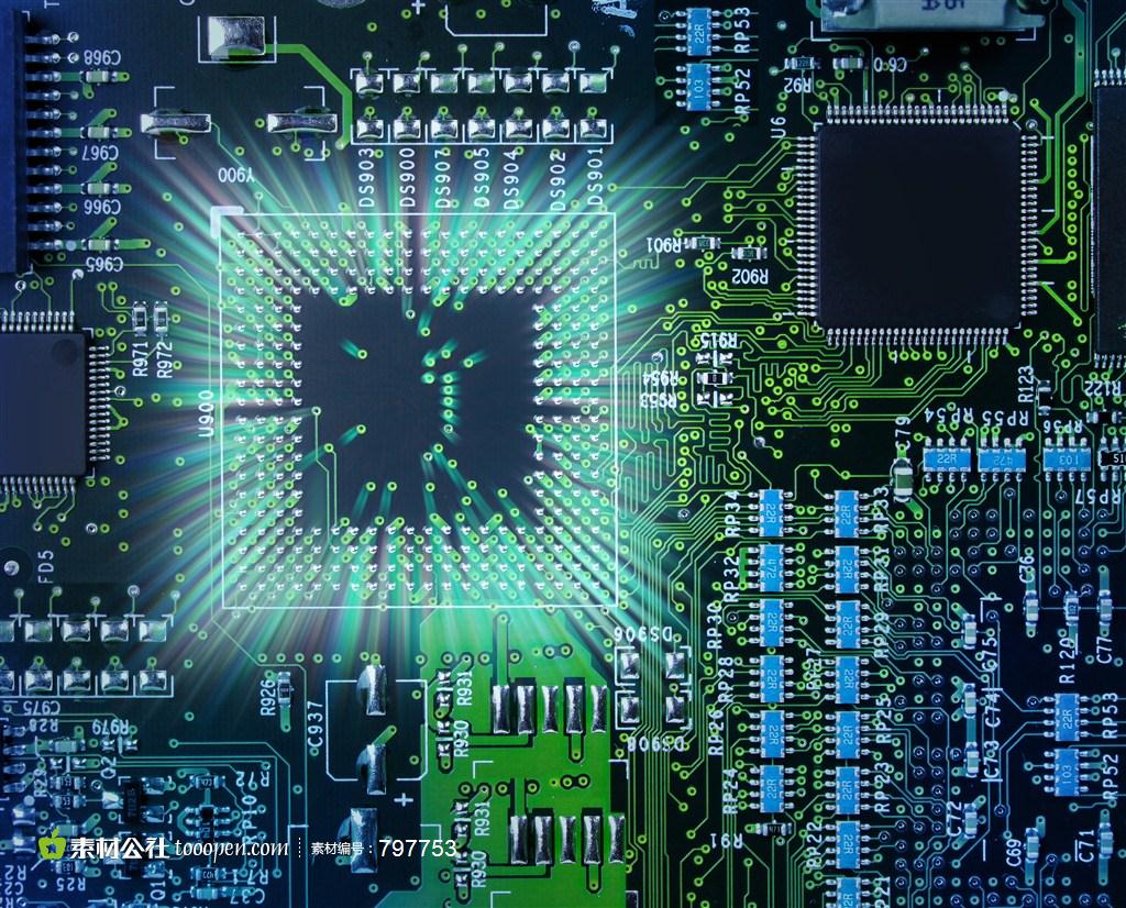
Printed circuit board

1. Visual inspection Visual inspection refers to visual inspection or use of some simple instruments, such as stereo microscope, metallographic microscope or even magnifying glass to inspect PCB board, find out the faulty parts and relevant physical evidence, and its main function is to locate the fault and make preliminary judgment on PCB Failure mode of the board Visual inspection mainly checks the PCB board for pollution, corrosion, explosion-proof board position, circuit wiring and fault rule, whether it is batch or single, whether it is always concentrated in a certain area, etc In addition, many PCB boards are found to be faulty after assembly. Whether the fault is caused by the assembly process and the influence of the data used in the process also need to carefully check the characteristics of the fault area
2. X-ray fluoroscopy inspection of some parts that cannot be inspected by visual inspection, as well as PCB board and other internal defects must be carried out by using X-ray fluoroscopy system The X-ray fluoroscopy system uses different principles of X-ray moisture absorption or transmissivity with different data thicknesses or different data densities for imaging This technology is more used to check the defect PCB A inside the welding joint, the internal defect of the through-hole of high-density packaging BGA or CSP devices and the positioning of defective solder joints At present, the resolution of industrial X-ray fluoroscopy equipment can reach 1 μ m or less, and is changing from two-dimensional imaging equipment to three-dimensional imaging equipment, and even five dimensional (5D) equipment is used for packaging inspection. However, this 5D X-ray optical fluoroscopy system is very expensive, and has few practical applications in industry
3. Slice analysis Slice analysis is to obtain PCB boards through a series of means and steps such as sampling, inlaying, slicing, polishing, corrosion, and observation Through slice analysis, rich information about microstructure reflects that the quality of PCB (through holes, electroplating, etc.) can be observed, which provides a good basis for the next step of quality improvement However, this method is destructive. Once sectioning is carried out, the sample will be destroyed; At the same time, this method requires a lot of sample preparation, which takes a long time and requires well-trained scientific and technical personnel to complete For detailed slicing process, you can refer to procedure 1.1 and IPC-MS-810 specified in IPC standard IPC-TM-650 2
The scanning acoustic microscope currently used for electronic packaging or assembly analysis is mainly a C-type ultrasonic scanning acoustic microscope, which uses amplitude and high-frequency ultrasound to reflect the phase and polarity changes generated on the discontinuous interface of data and images The scanning method is to scan the information in the XY plane along the Z axis Therefore, the scanning acoustic microscope can be used to detect various defects, data, and PCB s and PCB A in components, including cracks, delaminations, inclusions, and cavities If the frequency width of scanning acoustics is sufficient, internal defects in solder joints can also be directly detected The typical scanning acoustic image is red warning color, indicating the existence of defects Due to the use of a large number of plastic packaging components in the SMT process, a large number of problems are sensitive to moisture backflow during the conversion from lead to lead-free That is to say, when the lead-free process temperature is high, the hygroscopic plastic package will have internal or substrate delamination and cracking during the reflow process, and the ordinary PCB board will usually burst under the high temperature of the lead-free process In this regard, the scanning acoustic microscope highlights its special advantages in multi-layer high-density nondestructive testing PCB boards Generally obvious cracked plates can only be detected by visual appearance
5. Micro infrared analysis Micro infrared analysis is an analysis method combining infrared spectroscopy and microscope It uses the principle of different absorption of infrared spectroscopy by different materials (mainly organic substances) to analyze the compound composition of materials, and then combined with a microscope, visible light and infrared light are at the same optical path. As long as they are in the visible field of vision, trace organic pollutants to be analyzed can be found Without the combination of microscopes, infrared spectroscopy usually can only analyze samples with large sample size In many cases, in the field of electronic technology, trace contamination may lead to poor solderability of PCB pads or lead pins It can be imagined that without the infrared spectrometer to support the microscope, it is difficult to solve the process problem The main purpose of micro infrared analysis is to analyze the organic pollutants on the welding surface or solder joint surface, and analyze the causes of corrosion or poor weldability
6. Scanning Electron Microscope Analysis Scanning Electron Microscope (SEM) is a useful large-scale electron microscope imaging system for failure analysis. It working principle is to use the electron beam emitted by the camera to be accelerated by the anode and focus by a magnetic lens to form a beam The electron beam current with a diameter of tens to thousands of angstroms (A) The sample surface will stimulate various information, and after collection and amplification, various corresponding graphics can be obtained from the display screen The excited secondary electrons are generated within 5-10nm of the sample surface Therefore, secondary electrons can better reflect the surface morphology of the sample; The excited backscattered electrons are generated at 100 nm of the sample surface In the range of~1000nm, the backscattered electrons with different characteristics are emitted as substances with different atomic numbers. In summary, the backscattered electron image has the ability to distinguish the morphology and atomic number Therefore, the backscattered electron image can reflect the composition and distribution of chemical elements At present, the function of scanning electron microscope is very powerful. Any fine structure or surface feature can be magnified hundreds of thousands of times for observation and analysis
In terms of fault analysis, scanning electron microscopy is mainly used to analyze the failure mechanism of PCB or solder joints, especially to observe the morphology and structure of the pad surface, the metallographic structure of solder joints, measure intermetallic compounds, and solderability Coating analysis and tin whisker analysis and measurement, etc Unlike optical microscopes, scanning electron microscopes form electronic images, so there are only black and white. The samples of scanning electron microscopes need to conduct electricity, while non conductors and some transistors need to be sprayed with gold or carbon, otherwise charges will accumulate on the surface of the samples Observation of samples In addition, the image of scanning electron microscope is more profound than that of optical microscope. It is an important analysis method for inhomogeneous samples such as metallographic structure, microscopic fracture and tin whisker
7 X-ray energy spectrum analysis The scanning electron microscope is usually equipped with an X-ray energy spectrometer When the high-energy electron beam hits the sample surface, the internal electrons in the surface data atom are bombarded and escape, and the outer electrons transition to a lower energy level, which will excite the characteristic X-ray, which is a characteristic of the difference in energy levels of atoms of different elements X-rays are different. In retrospect, the characteristic X-rays emitted by the sample can be used as chemical components for analysis At the same time, the responding instruments are called spectral discrete spectrometer (impaired as spectrometer, WDS) and energy discrete spectrometer (impaired as energy spectrometer, EDS) according to the characteristic wavelength or energy of the detected X-ray signal The analysis speed of energy spectrometer is faster than that of spectrometer Due to its high speed and low cost, the universal scanning electron microscope is equipped with an energy spectrometer With different electron beam scanning methods, the energy spectrometer can perform point analysis, curve analysis and curve surface analysis, and obtain information about different element distributions Point analysis obtains all elements of the point; Line analysis executes one element analysis on the specified line each time, and scans multiple times to obtain the line distribution of all elements; Surface analysis analyzes all elements in the specified surface. The content of the measured elements is the average value of the measurement area In the analysis of PCB boards, the energy spectrometer is mainly used for the composition analysis of the pad surface, and the element analysis of contaminants on the pad and lead pin surfaces with poor solderability The quantitative analysis accuracy of the energy spectrometer is limited, and the content is less than 0.1%, which is usually not easy to detect The combination of energy spectrum and scanning electron microscope can obtain the information of surface morphology and composition at the same time, which is why they are widely used
8. When the photoelectron spectroscopy (XPS) sample is infrared by X-rays, the inner shell electrons of surface atoms will escape from the atomic nucleus and form electrons from the solid surface The kinetic energy Ex is measured, and the combination of atomic inner shell electrons can be obtained The energies Eb and Eb vary with the element and electron shell It is the atom's "fingerprint" identification parameter, and the formed spectrum line is the photoelectron spectrum (XPS) XPS can be used to perform qualitative and quantitative analysis of shallow surface (several nanometers) elements on the sample surface. In addition, information about chemical valence states of elements can be obtained from chemical shifts of binding energies It can provide information such as valence state of surface layer and bonding of surrounding elements; The incident beam is an X-ray photon beam, which can be used to analyze insulating samples without damaging the samples to be analyzed Rapid multi-element analysis; it can also be used in the case of argon ion stripping Longitudinal elemental distribution analysis of multilayers (see later) is performed with much higher sensitivity than energy dispersive spectroscopy (EDS). XPS is mainly used to analyze the quality of pad coating, pollution analysis and oxidation degree analysis to determine the deep causes of poor solderability of PCB
9. Thermal Analysis Differential Scanning Calorimetry (Differential Scanning Calorim - etry): A method of measuring the relationship between the power difference and temperature (or time) between the input material and the reference material under programmed temperature control DSC is equipped with two sets of compensating heating wires below the sample and reference containers Due to the thermal effect in the heating process, when there is a temperature difference between the sample and the reference, the differential thermal amplifier circuit and differential thermal compensation amplifier can be used, The relationship between the difference of the thermal power of the two electric heating compensations under the sample and the reference material with temperature (or time) changes DSC is widely used, but in analyzing PCB boards, it is mainly used to measure the curing degree of various polymer materials used on the surface PCB boards (such as Figure 2) and the glass transition temperature These two parameters determine the PCB Process reliability


Just upload Gerber files, BOM files and design files, and the KINGFORD team will provide a complete quotation within 24h.